はじめに
電気システムのサージ保護を指定する際、エンジニアは3つのコア技術、すなわち金属酸化物バリスタ(MOV)、ガス放電管(GDT)、およびトランジェント電圧サプレッサ(TVS)ダイオードの中から基本的な選択を迫られます。各技術は、異なる物理原理に基づく独自の性能特性を提供します。MOVは非線形セラミック抵抗を利用し、GDTはガス電離を利用し、TVSダイオードは半導体のアバランシェ降伏を利用します。.
選択は「最良」の技術を見つけることではありません。むしろ、基本的なトレードオフをアプリケーション要件に適合させることです。商用交流電源配線で優れるMOVは、高速データ回線では致命的に失敗する可能性があります。通信インターフェースに最適なGDTは、5V DC電源レールには不適切です。ボードレベルのI/Oに理想的なTVSダイオードは、雷に曝される屋外回路では無力かもしれません。.
本記事では、基本原理から各技術を検証し、性能差の背後にある物理を説明し、応答時間、クランプ電圧、エネルギー耐量、静電容量、経時特性、コストにわたる定量比較を提供します。配電システムを設計している場合でも、 SPD, 通信インターフェースの保護や多段保護の調整を行う際には、これらの根本的な違いを理解することが、調達を通過させるだけでなく、実際に保護機能を果たす部品を選択する上で役立ちます。.
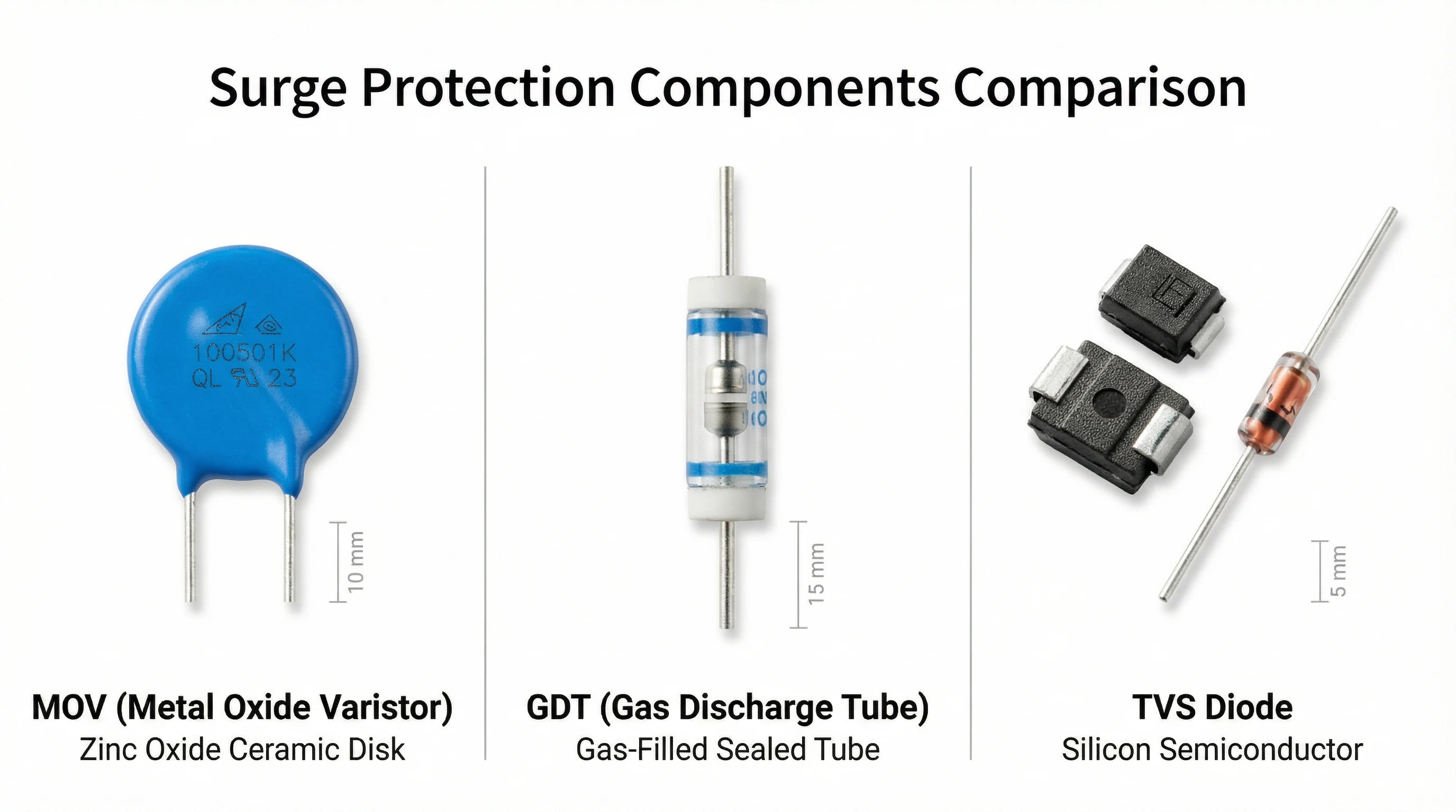
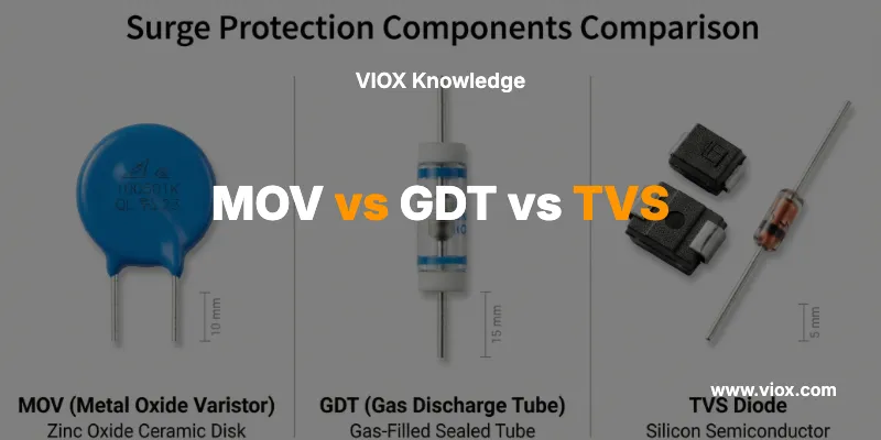
図0: 3種類のサージ保護技術の物理的比較。左: MOV(金属酸化物バリスタ)は、特徴的な青色の酸化亜鉛セラミックディスクとラジアルリード線を示しており、物理的なサイズは電圧定格(ディスクの厚さ)と電流容量(ディスクの直径)に比例します。中央: GDT(ガス放電管)は、不活性ガスと電極を封入した円筒形の密閉ガラス/セラミック容器を示しており、気密構造により安定した火花放電特性が保証されています。右: TVSダイオードは、コンパクトなSMD(0402、SOT-23)から大型のスルーホール形式(DO-201、DO-218)まで、様々な半導体パッケージを示しており、シリコンダイのサイズがパルス電力定格を決定します。これらの明確な物理的違いは、根本的に異なる動作原理を反映しています:セラミック粒界接合(MOV)、ガスイオン化プラズマ(GDT)、半導体アバランシェ降伏(TVS)。.
MOV(金属酸化物バリスタ):構造と動作原理
金属酸化物バリスタは、電圧が上昇すると抵抗が急激に低下するセラミック半導体デバイスです。この電圧依存性の挙動により、自動電圧クランプのように動作し、サージ時には強く導通しながら、通常動作時にはほとんど影響を与えません。.
内部構造
MOVは、酸化亜鉛(ZnO)粒子が少量のビスマス、コバルト、マンガン、その他の金属酸化物とともに焼結された構造を有する。その作用は粒界で発現する。隣接するZnO粒子間の各境界は微視的なショットキー障壁を形成し、実質的に微小な背中合わせダイオード接合として機能する。単一のMOVディスクには、複雑な三次元の直並列ネットワークで接続された数百万ものこのような微細接合が含まれている。.
このデバイスの巨視的特性は、その微細構造から生じる。ディスクの厚さは動作電圧を決定し(直列に並ぶ粒界が多いほど定格電圧が高くなる)、ディスクの直径は電流容量を決定する(並列経路が多いほどサージ電流耐量が高い)。このため、MOVのデータシートでは厚さ1mmあたりのバリスタ電圧が規定され、電力分配用の高エネルギーMOVは物理的に大型のブロックまたはディスクアセンブリとなる。.
動作原理
バリスタ電圧(Vᵥ)未満の電圧では、粒界接合は空乏モードを維持し、デバイスはマイクロアンペアレベルの漏れ電流のみを流す。サージにより電圧がVᵥを超えると、接合は量子トンネル効果となだれ増倍により降伏する。抵抗はメグオームからオームレベルまで急減し、MOVはサージ電流を接地側に分流する。.
この遷移は本質的に高速であり、材料レベルではサブナノ秒で生じる。標準的なカタログMOVの応答時間は25ナノ秒未満であり、これは主にリードインダクタンスとパッケージ形状によって制限され、ZnOの物理特性によるものではない。電圧-電流特性は高度に非線形であり、一般に I = K·Vᵅ の式で表される。非線形係数αは25から50の範囲にあり(線形抵抗のα = 1と比較)、その非線形性の高さを示している。.
主要仕様と動作特性
エネルギー耐量: MOVはサージエネルギーの吸収に優れる。メーカーはエネルギー耐量を2ミリ秒の矩形波パルスで、サージ電流耐量は標準的な8/20 µs波形で規定している。電力分配用のブロックMOVは、単一イベントで10,000~100,000アンペアのサージ電流を処理できる。.
経年劣化と性能低下: サージの反復曝露は累積的な微細構造損傷を引き起こす。バリスタ電圧は低下し、漏れ電流は増加し、クランプ性能は劣化する。過酷な過負荷は粒界を穿孔し、永久的な導通路を形成する可能性がある。このため、データシートには反復サージに対するデレーティング係数が規定され、重要な設備では保守パラメータとしてMOVの漏れ電流を監視すべきである。.
代表的な用途: AC電源系統のサージ保護、電力分配盤、産業用モータードライブ、重機、高速(ナノ秒)応答と高エネルギー吸収を必要とするあらゆる用途。.
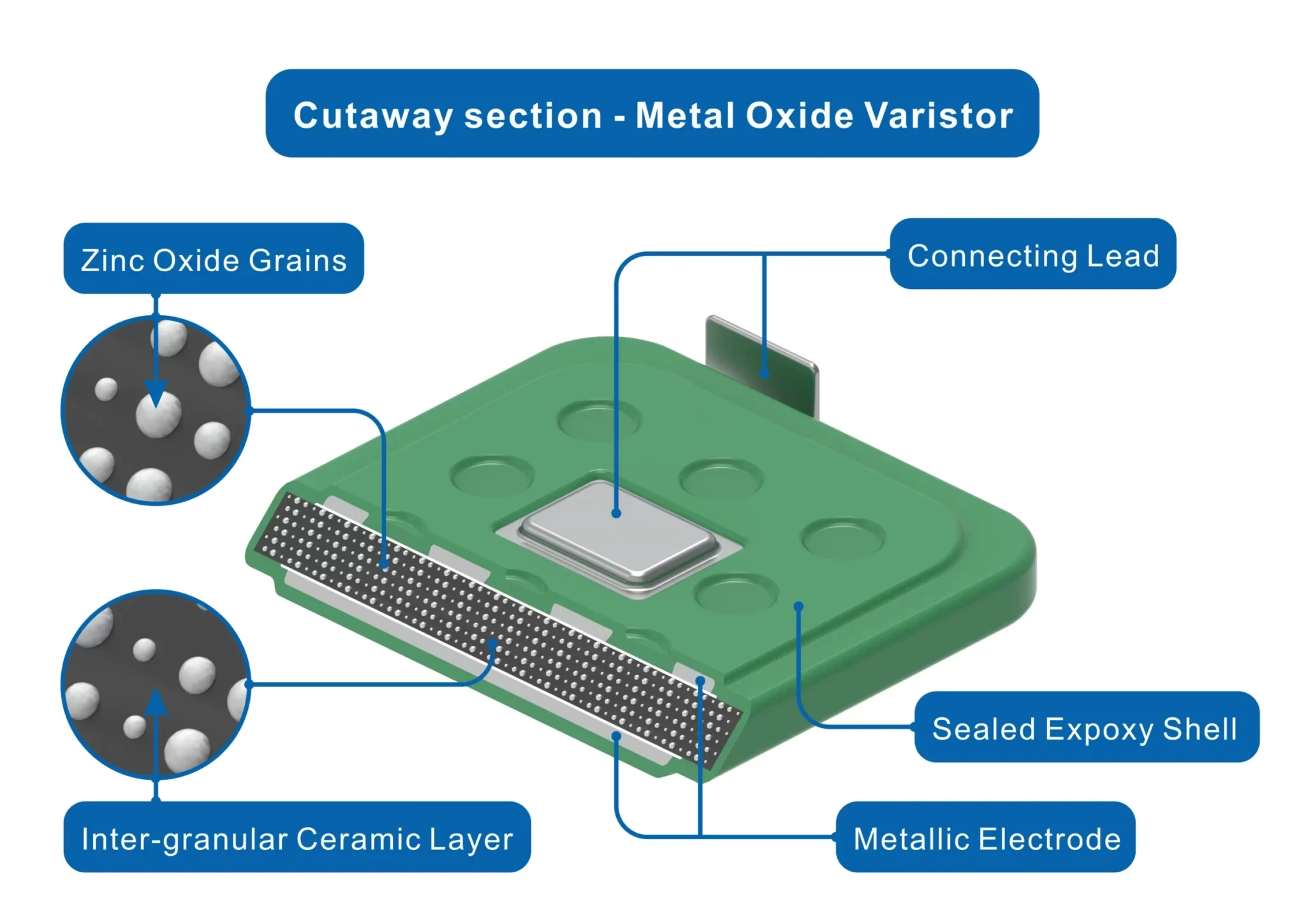
図1: MOVの断面図。セラミックマトリックスに埋め込まれた酸化亜鉛(ZnO)粒子と粒界(拡大図)を示す。各粒界は微視的なショットキー障壁を形成し、直並列構成で数百万の微細接合を生み出す。ディスクの物理的寸法——厚さは定格電圧を(直列粒界の数で)、直径は電流容量を(並列経路の数で)決定する——が、サージ保護性能を直接制御する。.
GDT(ガス放電管):構造と動作原理
ガス放電管は根本的に異なるアプローチを採用している:非線形抵抗による電圧クランプではなく、電圧が閾値を超えた時に一時的な短絡状態を作り出す。この「クラウバー」動作により、サージ電流は固体材料ではなく、イオン化したガスを通じて分流される。.
内部構造
GDTは、不活性ガス(通常はアルゴン、ネオン、またはキセノンの混合ガスを大気圧未満で封入)を充填したセラミックまたはガラス容器内に密封された2本または3本の電極で構成される。電極間ギャップとガス組成が降伏電圧を決定する。気密封止は極めて重要であり、汚染や圧力変化は降伏特性を変化させる。.
3電極GDTは通信アプリケーションで一般的であり、単一コンポーネントで線間保護と線対地保護を提供する。2電極タイプはより単純な線対地構成に用いられる。電極は、降伏電圧を低減しアーク形成を安定化させる材料でコーティングされることが多い。.
動作原理
通常状態では、ガスは非導電性であり、GDTは極めて低い容量(通常2ピコファラド以下)で、ほぼ無限大のインピーダンス(>10⁹ Ω)を示す。過渡電圧が火花放電開始電圧を超えると、電界によりガスがイオン化される。自由電子が加速されガス原子と衝突し、なだれ過程でさらに多くの電子を放出する。1マイクロ秒未満のうちに、電極間に導電性プラズマチャネルが形成される。.
一旦イオン化すると、GDTはアークモードに移行する。デバイス両端の電圧は低いアーク電圧(通常10~20ボルト)まで低下し、初期の降伏電圧に関わらずこの値を維持する。デバイスはほぼ短絡状態として機能し、サージ電流をプラズマを通じて分流する。アークは、電流が「グロー放電からアーク放電への遷移電流」(通常数十ミリアンペア)を下回るまで持続する。.
このクローバー動作は、重要な設計上の考慮事項を生み出します。保護された回路がグロー閾値を超える十分な「フォロー電流」を供給できる場合、GDTは過渡現象が終了した後でも導通を維持する可能性があります。これが、AC主電源のGDTが直列抵抗または上流のブレーカーとの連携を必要とする理由です。低インピーダンスのDC電源では、フォロー電流のラッチングは壊滅的なものになる可能性があります。.
主要仕様と動作特性
サージ電流耐量:GDTは非常に高いサージ電流を処理します。一般的な通信グレードのデバイスは、10,000〜20,000アンペア(8/20 µs波形)の定格で、マルチショット耐久性を備えています。この高い容量は、局所的な固体接合ではなく、プラズマチャネルの分散された性質に由来します。.
静電容量:GDTの決定的な利点は、2 pF未満の静電容量であり、高速信号に対して透過的であることです。これが、xDSL、ケーブルブロードバンド、ギガビットイーサネットがMOVまたは多くのTVSデバイスの静電容量を許容できないため、GDTが通信回線保護を支配している理由です。.
応答時間:GDTは、固体デバイスよりも低速です。ブレークダウンは通常、数百ナノ秒から数マイクロ秒以内に発生します。これは、電圧オーバーシュートによって異なります(dV/dtが高いほど、イオン化が加速されます)。敏感な電子機器の高速トランジェントの場合、GDTは多くの場合、連携された保護スキームでより高速なクランプと組み合わされます。.
安定性と寿命:高品質のGDTは、優れた長期安定性を示します。ITU-T K.12およびIEEE C62.31テスト方法は、数千回のサージサイクルにわたるパフォーマンスを検証します。UL認定の通信GDTは、数十年にわたるサービスで最小限のパラメータシフトを示します。.
代表的な用途:通信回線保護(xDSL、ケーブル、光ファイバー)、高速イーサネットインターフェイス、RFおよびアンテナ入力、および最小限の回線負荷が不可欠であり、サージ源インピーダンスがフォロー電流のラッチングを防ぐのに十分な高さであるアプリケーション。.
図2:ガス放電管(GDT)の構造と動作。左の図は内部構造を示しています。電極ギャップと不活性ガス(アルゴン/ネオン)が充填された密閉ガスチャンバー。右のグラフはイオン化応答を示しています。過渡電圧がスパークオーバー閾値を超えると、ガスがイオン化して導電性プラズマチャネルが作成され、電圧がアークモード(〜10〜20V)に低下し、電流がグローからアークへの遷移閾値を下回るまで、サージ電流がプラズマを介して分流されます。.
TVSダイオード:構造と動作原理
過渡電圧サプレッサダイオードは、サージクランプ用に特別に設計されたシリコンアバランシェデバイスです。これらは、サージ保護コンポーネントで利用可能な最速の応答時間と最低のクランプ電圧を組み合わせているため、敏感な半導体回路の保護に最適な選択肢です。.
内部構造
TVSダイオードは、基本的に、電圧調整ではなく、高パルス電力用に最適化された特殊なツェナーダイオードです。シリコンダイは、正確な電圧でアバランシェブレークダウンに入るように設計された、高ドープされたP-N接合を備えています。ダイ面積は、サージイベントのピーク電流(サブマイクロ秒パルスで数百アンペア)を処理するために、同等のツェナーレギュレーターよりもはるかに大きくなっています。.
動作原理
通常の動作電圧では、TVSダイオードはナノアンペアレベルのリークのみで逆バイアスで動作します。トランジェントが逆ブレークダウン電圧(V_BR)を超えると、シリコン接合がアバランシェ増倍に入ります。衝撃イオン化により、電子-正孔ペアが大量に生成され、接合抵抗が低下します。デバイスは、ブレークダウンレベルに動的抵抗とサージ電流を掛けた電圧で電圧をクランプします。.
物理学は完全に固体であり、機械的な動き、ガスイオン化、または材料の相変化はありません。これにより、ナノ秒範囲での応答時間が可能になります。ベアシリコンの場合は1 ns未満ですが、パッケージインダクタンスにより、実用的なデバイスの場合は通常1〜5 nsに効果的な応答がプッシュされます。電圧-電流特性は非常に急峻(低い動的抵抗)であり、タイトなクランプを提供します。.
主要仕様と動作特性
パルス電力定格:TVSメーカーは、標準化されたパルス幅(通常は10/1000 µsの指数波形)を使用して電力容量を指定します。一般的な製品ファミリーは、400W、600W、1500W、または5000Wのパルス定格を提供します。ピーク電流容量は、パルス電力とクランプ電圧から計算されます。15Vクランプの600Wデバイスは約40Aのピークを処理します。.
クランプ性能:TVSダイオードは、あらゆるサージ保護技術の中で最も低いクランプ電圧を提供します。クランプ電圧とスタンドオフ電圧の比率(V_C/V_WM)は、通常1.3〜1.5ですが、MOVの場合は2.0〜2.5です。この厳密な制御は、3.3Vロジック、5V USB、12V車載回路、およびその他の電圧に敏感な負荷を保護するために重要です。.
静電容量:TVS静電容量は、デバイスの構造によって大きく異なります。標準の接合TVSダイオードは数百ピコファラッドを示す可能性があり、高速データラインをロードします。HDMI、USB 3.0、イーサネット、およびRF用に設計された低静電容量TVSファミリーは、特殊な接合形状を使用し、ラインあたり5 pF未満を実現します。.
経年劣化と信頼性:MOVとは異なり、TVSダイオードは、定格パルスストレス下で最小限の性能ドリフトを示します。シリコン接合は、定格内の繰り返しのサージから累積的に劣化しません。故障モードは通常、開回路(接合消滅)または短絡(金属化溶融)であり、どちらも定格を大幅に超える極端な過負荷でのみ発生します。.
代表的な用途:ボードレベルの回路保護(I/Oポート、電源レール)、USBおよびHDMIインターフェイス、車載電子機器、DC電源、通信データライン、および半導体負荷の高速応答とタイトな電圧クランプを必要とするアプリケーション。.
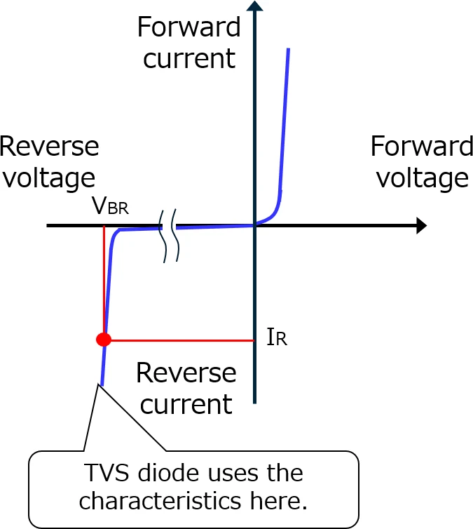
図3:半導体アバランシェ動作を示すTVSダイオードの電圧-電流(I-V)特性曲線。通常の電圧(V_WMスタンドオフ領域)では、デバイスはナノアンペアリークで高いインピーダンスを維持します。トランジェントが逆ブレークダウン電圧(V_BR)を超えると、シリコンP-N接合がアバランシェ増倍に入ります。接合抵抗が低下し、デバイスはV_C(ブレークダウン電圧+動的抵抗×サージ電流)で電圧をクランプします。急峻な曲線(低い動的抵抗)は、半導体負荷の保護に不可欠な厳密な電圧制御を提供します。.
クランプ対クローバー:2つの保護哲学
これらのテクノロジーの根本的な違いは、その保護哲学にあります。MOVとTVSダイオードは クランプデバイス—サージ電流に比例する特定のレベルに電圧を制限します。GDTは クローバーデバイス—電流の大きさに関係なく、電圧を低い残留レベルに低下させる短絡回路を作成します。.
クランプ動作 (MOVおよびTVS):サージ電流が増加すると、デバイスの非線形V-I曲線に従ってクランプ電圧が上昇します。275V RMSの定格のMOVは、1 kAのサージで750Vでクランプする可能性がありますが、5 kAで900Vまで上昇します。15Vスタンドオフの定格のTVSダイオードは、10Aで24Vでクランプする可能性がありますが、20Aで26Vに達します。保護された負荷は、サージ振幅とデバイスの特性によって決定される電圧を受けます。.
クローバー動作 (GDT):ブレークダウンが発生すると、GDTはアークモードに入り、サージ電流が100Aであろうと10,000Aであろうと、電圧は10〜20Vに低下します。これにより、トリガーされると優れた保護が提供されますが、初期のスパークオーバーにより、イオン化が完了する前に電圧スパイクが発生する可能性があります。これが、GDTの背後にある敏感な負荷が、多くの場合、二次的な高速クランプを必要とする理由です。.
各哲学は、さまざまなアプリケーションに適しています。クランプデバイスは、電圧への露出を制限することにより保護します。クローバーデバイスは、電流を分流することにより保護します。クランプは、保護された回路がクランプ電圧を許容できる場合に機能します。クローバーは、サージ源のインピーダンスが十分に高く、ラインを短絡しても上流の機器が損傷したり、フォロー電流の問題が発生したりしない場合に機能します。.
MOV vs GDT vs TVS:並べて比較
以下の表は、これら3つのサージ保護テクノロジー全体の主要なパフォーマンスの違いを定量化したものです。
| パラメータ | MOV(金属酸化物バリスタ) | GDT(ガス放電管) | TVSダイオード |
| 動作原理 | 電圧依存性非線形抵抗(ZnO粒界) | ガスイオン化クローバー | 半導体アバランシェブレークダウン |
| 保護メカニズム | クランプ | クローバー | クランプ |
| 応答時間 | <25 ns(一般的なカタログ部品) | 100 ns〜1 µs(電圧依存) | 1〜5 ns(パッケージ制限) |
| クランプ/アーク電圧 | 2.0〜2.5 × MCOV | 10〜20 V(アークモード) | 1.3〜1.5 × V_standoff |
| サージ電流(8/20 µs) | 400 A〜100 kA(サイズ依存) | 5 kA〜20 kA(通信グレード) | 10 A〜200 A(600Wファミリー〜40A) |
| エネルギー耐量 | 優秀(100〜1000 J) | 優秀(分散プラズマ) | 中程度(接合部によって制限される) |
| 静電容量 | 50-5000 pF (面積依存) | <2 pF | 5-500 pF (構造依存) |
| 経年変化 | サージサイクルで劣化; V_nがドリフトダウン | 数千回のサージに対して安定 | 定格内で最小限のドリフト |
| 故障モード | 劣化 → 短絡または開放 | 短絡 (アーク維持) | 開放または短絡 (壊滅的な場合のみ) |
| フォロー電流リスク | 低 (自己消弧) | 高 (外部制限が必要) | なし (ソリッドステート) |
| 標準的な電圧範囲 | 18V RMS – 1000V RMS | 75V – 5000V DCスパークオーバー | 3.3V – 600Vスタンドオフ |
| コスト (相対) | 低 ($0.10 – $5) | 低~中 ($0.50 – $10) | 低~中 ($0.20 – $8) |
| 規格 | IEC 61643-11, UL 1449 | ITU-T K.12, IEEE C62.31 | IEC 61643-11, UL 1449 |
| 主な用途 | AC主電源、配電、産業用 | 通信回線、高速データ、アンテナ | ボードレベルI/O、DC電源、自動車 |
比較からの重要なポイント
MOV は、電力レベルのサージに対して、エネルギー処理、高速応答、およびコストの最適なバランスを提供します。AC主電源保護で優位を占めていますが、高周波回路での静電容量負荷と、繰り返しのストレス下での累積的な経年劣化に悩まされます。.
GDT は、ライン負荷を最小限に抑えることが重要であり、サージ電流容量を最大化する必要がある場合に優れています。超低静電容量により、通信およびRFアプリケーションではかけがえのない存在ですが、応答の遅さとフォロー電流のリスクには、慎重な回路設計が必要です。.
TVSダイオード は、敏感な電子機器に最も高速で厳密なクランプを提供します。50V未満の電圧で半導体I/Oを保護するための唯一の実用的な選択肢ですが、エネルギー容量が限られているため、MOVやGDTが日常的に吸収する雷レベルのサージを処理できません。.
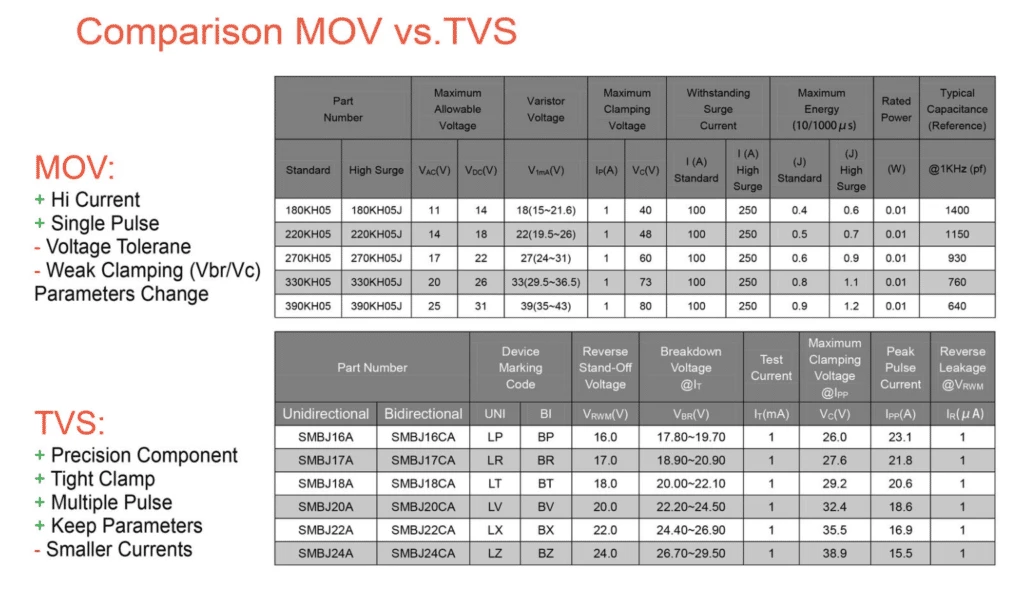
図4:主要な仕様にわたるMOV(金属酸化物バリスタ)およびTVS(過渡電圧サプレッサ)技術を対比する専門的な比較チャート。MOVは、電力レベルのサージに対して優れたエネルギー吸収を備えた、より高いクランプ電圧比(2.0〜2.5×MCOV)を示しますが、TVSダイオードは、半導体保護のために、より高速な応答(<5 ns)で、より厳密な電圧制御(1.3〜1.5×スタンドオフ)を提供します。この表には、電圧定格、サージ電流容量、および各技術の相補的な性能範囲を示す標準的な部品番号の例が含まれています。.
技術選択ガイド:それぞれの使用時期
適切なサージ保護技術の選択は、デバイスの特性を回路要件に一致させることに依存します。以下に、意思決定のフレームワークを示します。
MOVの使用時期:
- 回路電圧がAC主電源または高電圧DC(> 50V)の場合:MOVは、18V RMSから1000Vを超える電圧定格で利用可能であり、住宅(120 / 240V)、商業(277 / 480V)、および産業用配電に完全に適合します。.
- サージエネルギーが高い場合:雷によるサージ、ユーティリティのスイッチング過渡現象、およびモーターの突入電流は、MOVのみが経済的に吸収できるエネルギーレベル(数百から数千ジュール)を生成します。.
- 応答時間<25 nsが許容される場合:ほとんどのパワーエレクトロニクスおよび産業機器は、MOVの応答速度を許容します。.
- 静電容量負荷が許容される場合:電力周波数(50/60 Hz)では、1000 pFの静電容量でさえ無視できます。.
- コストが制約されている場合:MOVは、ジュールあたりの保護コストが最も低くなります。.
MOVを避けるべき場合 高速通信回線(静電容量負荷)、低電圧半導体回路(クランプ電圧が高すぎる)、または数十年にわたってドリフトのない性能が保証されるアプリケーション(経年劣化の懸念)を保護する場合。.
GDTの使用時期:
- ライン負荷を最小限に抑える必要がある場合(<2 pF):xDSLモデム、ケーブルブロードバンド、ギガビットイーサネット、RFレシーバー、およびアンテナ入力は、MOVまたは標準のTVSデバイスの静電容量を許容できません。.
- サージ電流容量を最大化する必要がある場合:通信中央局、携帯電話基地局、および屋外設備は、TVS定格を超える、繰り返しの高振幅雷サージに直面します。.
- 保護された回路のソースインピーダンスが高い場合:電話回線(600Ω)、アンテナフィーダーライン(50-75Ω)、およびデータケーブルは、過度のフォロー電流なしに安全にクローバーできます。.
- 動作電圧が高い場合(> 100V):GDTは、75Vから5000Vのスパークオーバー電圧で利用可能であり、通信電圧、PoE(Power over Ethernet)、および高電圧信号をカバーします。.
GDTを避けるべき場合 低インピーダンスDC電源(フォロー電流のリスク)、最速の応答(<100 nsが重要)を必要とする回路、または初期のスパークオーバーピークを許容できない電圧に敏感な負荷(二次クランプが必要)を保護する場合。.
TVSダイオードの使用時期:
- クランプ電圧を厳密に制御する必要がある場合3.3Vロジック、5V USB、12V車載回路、およびその他の半導体負荷は、公称電圧の20〜30%以内でクランプする必要があります—これを実現できるのはTVSダイオードのみです。.
- 応答時間は最速である必要があります(<5 ns)高速プロセッサ、FPGA、および高感度アナログ回路の保護には、ナノ秒単位の応答が必要です。.
- 回路電圧は低〜中程度です(<100V)TVSファミリは、3.3Vデータラインから48Vテレコム電源まで、あらゆるものをカバーします。.
- 経年劣化/ドリフトは許容できません医療機器、航空宇宙、および安全が重要なシステムでは、製品寿命にわたって予測可能で安定した保護が必要です。.
- 基板スペースは限られています0402またはSOT-23パッケージのSMT TVSデバイスは、MOVおよびGDTが適合しない場所に適合します。.
以下の場合、TVSダイオードの使用は避けてください サージエネルギーがパルス電力定格を超える場合(一般的な600Wデバイスは〜1ジュールしか吸収しません)、サージ電流がピーク定格を超える場合(15Vで600Wの場合、通常40A)、またはマルチラインシステムでチャネルあたりのコストが法外になる場合。.
決定マトリックス
| の応用 | 主要技術 | 根拠 |
| AC主電源パネル保護 | MOV(Type 1/2 SPD) | 高エネルギー、120〜480V、費用対効果が高い |
| テレコム回線インターフェース | GDT + TVS(段階的) | GDTがエネルギーを吸収し、TVSが残留電圧をクランプします |
| USB 2.0 / 3.0データライン | 低容量TVS | 高速エッジ、5V電源、<5 pFが必要 |
| イーサネット(10/100/1000 Base-T) | GDT(一次)+低容量TVS | 最小限の負荷、高いサージ暴露 |
| 24V DC産業用I/O | TVS | タイトなクランプ、高速応答、経年劣化なし |
| PVソーラーDC入力 | MOV(DC定格) | 高電圧(600〜1000V)、高エネルギー |
| 車載12V回路 | TVS | 負荷ダンプ保護、24〜36Vでのタイトなクランプ |
| RFアンテナ入力 | GDT | 2 pF未満、高電力処理 |
| 3.3V FPGA電源レール | TVS(低容量) | 6〜8Vクランプ、<1 nsの応答が重要 |
このマトリックスは出発点です。複雑な設置では、多くの場合、多層保護スキームでテクノロジーを組み合わせ、各段階の強みを活用します。.
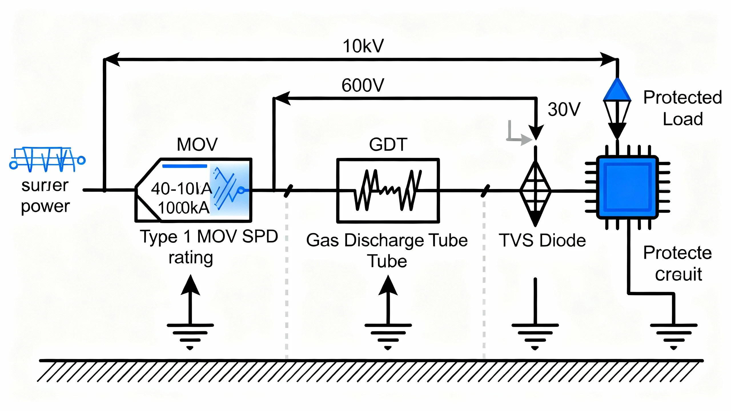
図5:連携された保護戦略を示す、プロフェッショナルな3段階サージ保護アーキテクチャ図。ステージ1(一次):サービスエントランスのType 1 MOV SPDは、極端なサージエネルギー(40〜100 kA)を処理し、電圧を10+ kVから〜600Vにクランプします。ステージ2(二次):ガス放電管は、残留高電圧トランジェントを分流し、アークモード動作により電圧を〜30Vに低減します。ステージ3(最終):TVSダイオードは、高感度半導体負荷を保護するために、ナノ秒単位の応答でタイトなクランプ(<1.5×スタンドオフ電圧)を提供します。各ステージは、適切な接地と電圧調整を備えており、上流のデバイスが下流のコンポーネントよりも先にトリガーされるようにし、保護カスケード全体にサージエネルギーを分散する明確な「ハンドオフ」ポイントを作成します。この多層アプローチは、MOV(高エネルギー)、GDT(低容量)、およびTVS(タイトなクランプ)テクノロジーの相補的な強みを活用します。.
多層保護:テクノロジーの組み合わせ
最も堅牢なサージ保護アーキテクチャは、単一のテクノロジーに依存していません。代わりに、複数のステージを連携させ、それぞれが脅威スペクトルの異なる部分に最適化されています。この「多層防御」アプローチは、MOV、GDT、およびTVSテクノロジーの相補的な強みを活用します。.
なぜ多層保護が必要なのか?
エネルギー分散単一のTVSダイオードは10 kAの雷サージを吸収できませんが、上流のGDTはそのエネルギーの99%を分流し、TVSが残留電圧をクランプできるようにします。各ステージは、最も得意なことを処理します。.
速度の最適化GDTがイオン化するには数百ナノ秒かかります。その間、下流の高速TVSは初期スパイクをクランプし、高感度負荷への損傷を防ぐことができます。GDTが発火すると、バルク電流の分流を引き継ぎます。.
電圧調整上流のデバイスは、下流のデバイスよりも先にブレークダウンする必要があります。適切な選択により、最初のステージがたとえば600Vで導通し、2番目のステージ(定格150V)に到達するものを制限し、次に最終負荷(定格50V)を保護します。.
一般的な多層アーキテクチャ
テレコムインターフェース(GDT + TVS):
- 一次ステージインターフェース境界のGDTは、直接雷撃および高電圧電力障害(2〜10 kVサージ、最大20 kA)を処理します。.
- 二次ステージ低容量TVSダイオードは、残留トランジェントをトランシーバーICの安全なレベル(<30V)にクランプします。.
- コーディネーションGDTのスパークオーバーは400V、TVSのブレークダウンは15V、トランシーバーの最大定格は12Vです。TVSはGDTのイオン化遅延中に保護します。GDTが発火すると、バルク電流の役割を引き継ぎます。.
イーサネットPoE(GDT + TVS +インダクタ):
- 一次GDTは、ライン-グラウンド雷サージを分流します。.
- 直列インダクタサージの立ち上がり時間(dV/dt)を遅らせ、GDTがイオン化する時間を与え、下流ステージへの電流を制限します。.
- 二次各差動ペアのTVSダイオードは、コモンモードおよび差動モードのトランジェントをクランプし、イーサネットPHY(±8V max)を保護します。.
産業用ACパネル(MOV一次+ MOV二次):
- サービス・エントランス: タイプ1 MOVは40〜100 kAの定格で、直撃雷に対応します(IEC 61643-11に準拠した1.2/50 µsの電圧、10/350 µsの電流波形)。.
- 分電盤: タイプ2 MOVは20〜40 kAの定格で、建物配線を介して結合する残留サージを抑制します。.
- 負荷機器: タイプ3 SPDまたは基板レベルのTVSは、最終的な使用点保護を提供します。.
PVソーラーシステム(MOV DC + TVS):
- アレイ接続箱: PVストリング出力のDC定格MOV(600〜1000V)は、雷誘導サージに対応します。.
- インバーター入力: TVSダイオードは、DC-DCコンバーターおよびMPPTコントローラーの半導体を保護し、シリコンが耐えられるレベルでクランプします。.
連携を成功させるための鍵は、明確な「引き継ぎ」ポイントを作成する降伏電圧を選択し、ある段階からの通過エネルギーが次の段階の定格範囲内にとどまることを検証することです。完全なSPDシステム(VIOXなど)のメーカーは、この設計の複雑さを排除する、テスト済みの連携アセンブリを公開することがよくあります。.
結論
サージ保護コンポーネントの選択は、「最高の」テクノロジーを見つけることではなく、物理的特性を要件に適合させることです。MOVは酸化亜鉛セラミックを利用して、電力電圧で高エネルギーを吸収します。GDTはガス電離を利用して、最大の電流容量で最小限のライン負荷を実現します。TVSダイオードは、半導体アバランシェを利用して、最も高速で厳密な機密電子機器のクランプを実現します。.
各テクノロジーは、基本的なトレードオフを表しています。
- MOVは、優れたエネルギー処理能力とコストのために、より高いクランプ電圧と経年劣化をトレードオフします。.
- GDTは、超低静電容量とサージ耐久性のために、より遅い応答とフォロー電流のリスクをトレードオフします。.
- TVSダイオードは、最も高速な応答と最も厳密な電圧制御のために、限られたエネルギー容量をトレードオフします。.
検討した動作原理に根ざしたこれらのトレードオフを理解することで、アプリケーションで実際に機能する保護を指定できます。5Vデータラインの600V MOVは保護に失敗します。10 kAの雷サージに直面した40A TVSダイオードは、壊滅的に故障します。低インピーダンスDC電源のGDTは、破壊的なフォロー電流伝導にラッチする可能性があります。.
複雑な設置の場合、多層保護は複数のテクノロジーを連携させ、それぞれが最高のパフォーマンスを発揮する場所に配置します。GDTはバルクエネルギーを吸収し、MOVは電力レベルのサージを処理し、TVSは半導体負荷の最終段階のクランプを提供します。.
IEC 61643-11に準拠した100 kAの定格の配電SPDを設計する場合でも、2 pF未満の負荷でギガビットイーサネットインターフェイスを保護する場合でも、3.3V FPGA I/Oを保護する場合でも、意思決定のフレームワークは同じです。デバイスの物理的特性を回路要件に適合させ、脅威波形に対する定格を検証し、単一のテクノロジーがスペクトル全体をカバーできない場合は、段階を連携させます。.
VIOXについて: サージ保護デバイスの大手メーカーとして、VIOXは、住宅、商業、および産業アプリケーション向けの包括的なMOV、GDT、およびTVSソリューションを提供しています。当社のエンジニアリングチームは、連携保護システムのアプリケーションサポートを提供します。アクセス www.viox.com または、仕様に関するサポートについては、当社の技術営業チームにお問い合わせください。.