소개
전기 시스템에 서지 보호를 지정할 때, 엔지니어는 세 가지 핵심 기술(Metal Oxide Varistor(MOV), Gas Discharge Tube(GDT), Transient Voltage Suppressor(TVS) 다이오드) 중에서 근본적인 선택을 직면합니다. 각 기술은 서로 다른 물리적 원리에 기반한 독특한 성능 특성을 제공합니다—MOV는 비선형 세라믹 저항을 활용하고, GDT는 가스 이온화를 이용하며, TVS 다이오드는 반도체 애벌랜치 항복을 활용합니다.
선택은 “최고”의 기술을 찾는 문제가 아닙니다. 오히려 근본적인 절충점을 애플리케이션 요구사항에 맞추는 문제입니다. AC 전원 배전에서 뛰어난 MOV가 고속 데이터 라인에서는 치명적으로 실패할 수 있습니다. 통신 인터페이스에 완벽한 GDT는 5V DC 공급 레일에 적합하지 않을 것입니다. 보드 레벨 I/O에 이상적인 TVS 다이오드는 낙뢰에 노출된 옥외 회로에서는 압도될 수 있습니다.
본 기사는 각 기술을 기본 원리부터 검토하고, 성능 차이 뒤에 숨은 물리를 설명하며, 응답 시간, 클램핑 전압, 에너지 처리량, 커패시턴스, 노화 특성 및 비용에 걸쳐 정량적 비교를 제공합니다. 전원 배전을 설계하든, SPD, 통신 인터페이스를 보호하든, 다단 보호를 조정하든, 이러한 근본적인 차이를 이해하면 단순히 구매 조건을 통과하는 것이 아니라 실제로 보호하는 부품을 선택하는 데 도움이 될 것입니다.
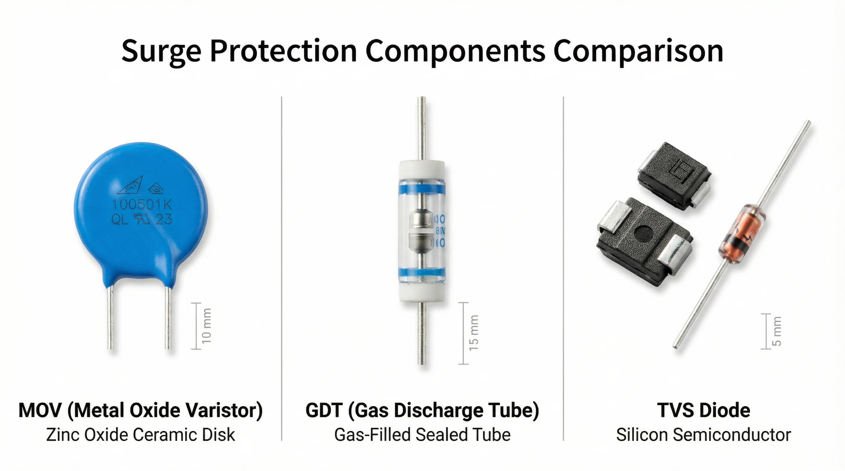
그림 0: 세 가지 서지 보호 기술의 물리적 비교. 왼쪽: MOV(Metal Oxide Varistor)는 방사형 리드가 있는 특징적인 청색 산화아연 세라믹 디스크를 보여줍니다—물리적 크기는 정격 전압(디스크 두께) 및 전류 용량(디스크 직경)에 따라 비례합니다. 중앙: GDT(Gas Discharge Tube)는 불활성 가스와 전극을 포함한 원통형 밀봉 유리/세라믹 외피를 보여줍니다—기밀 구조는 안정적인 스파크오버 특성을 보장합니다. 오른쪽: TVS 다이오드는 컴팩트 SMD(0402, SOT-23)부터 더 큰 스루홀 형식(DO-201, DO-218)까지 다양한 반도체 패키지를 보여줍니다—실리콘 다이 크기가 펄스 전력 정격을 결정합니다. 이러한 현격한 물리적 차이는 근본적으로 다른 동작 원리(세라믹 입자 경계 접합(MOV), 가스 이온화 플라즈마(GDT), 반도체 애벌랜치 항복(TVS))를 반영합니다.
MOV(Metal Oxide Varistor): 구조 및 동작 원리
금속 산화 바리스터는 전압이 증가함에 따라 저항이 급격히 떨어지는 세라믹 반도체 소자입니다. 이 전압 의존적 동작은 자동 전압 클램프처럼 작동하게 합니다—서지 시에는 강하게 전도를 하면서 정상 동작 시에는 거시적으로 보이지 않습니다.
내부 구조
MOV는 소량의 비스무트, 코발트, 망간 및 기타 금속 산화물과 함께 소결된 산화아연(ZnO) 입자로 구성됩니다. 마법은 입자 경계에서 일어납니다. 인접한 ZnO 입자 사이의 각 경계는 미세한 쇼트키 장벽—본질적으로 아주 작은 백투백 다이오드 접합—을 형성합니다. 단일 MOV 디스크에는 복잡한 3차원 직병렬 네트워크로 연결된 수백만 개의 이러한 미세 접합이 포함됩니다.
소자의 전체적 특성은 이 미세 구조에서 나타납니다. 디스크 두께는 동작 전압을 결정합니다(직렬로 연결된 입자 경계가 많을수록 = 더 높은 정격 전압). 디스크 직경은 전류 용량을 결정합니다(병렬 경로가 많을수록 = 더 높은 서지 전류). 이것이 MOV 데이터시트가 두께 1mm당 바리스터 전압을 지정하고, 전원 배전용 고에너지 MOV가 물리적으로 큰 블록 또는 디스크 어셈블리인 이유입니다.
운영 원칙
바리스터 전압(Vᵥ) 미만의 전압에서는 입자 경계 접합이 공핍 모드로 유지되며 소자는 마이크로암페어 수준의 누설 전류만 흡수합니다. 서지가 전압을 Vᵥ 이상으로 올리면, 접합은 터널링 및 애벌랜치 증배를 통해 항복합니다. 저항은 메그옴에서 옴으로 급락하며, MOV는 서지 전류를 접지로 분로합니다.
이 전환은 본질적으로 빠릅니다—물질 수준에서는 나노초 미만입니다. 표준 카탈로그 MOV는 주로 리드 인덕턴스와 패키지 형상에 의해 제한되며, ZnO 물리 자체보다는 25나노초 미만의 응답 시간을 달성합니다. 전압-전류 특성은 매우 비선형이며, 일반적으로 I = K·Vᵅ 방정식으로 설명됩니다. 여기서 비선형 계수 α는 25에서 50 범위입니다(선형 저항기의 α = 1과 비교).
주요 사양 및 동작
에너지 처리량: MOV는 서지 에너지를 흡수하는 데 탁월합니다. 제조사는 2밀리초 직사각형 펄스로 에너지 용량을, 표준 8/20 µs 파형으로 서지 전류를 정격화합니다. 전원 배전용 블록 MOV는 단일 사건에서 10,000~100,000 암페어의 서지 전류를 처리할 수 있습니다.
노화 및 성능 저하: 반복적인 서지 노출은 누적적인 미세 구조 손상을 유발합니다. 바리스터 전압은 하향 이동하고, 누설 전류는 증가하며, 클램핑 성능은 저하됩니다. 심한 과부하는 입자 경계를 관통하여 영구적인 전도 경로를 생성할 수 있습니다. 이러한 이유로 데이터시트는 반복 서지에 대한 디레이팅 계수를 지정하며, 중요한 설비에서는 유지 보수 파라미터로 MOV 누설 전류를 모니터링해야 합니다.
일반적인 애플리케이션: AC mains surge protection, power distribution panels, industrial motor drives, heavy equipment, and any application requiring high energy absorption with fast (nanosecond) response.
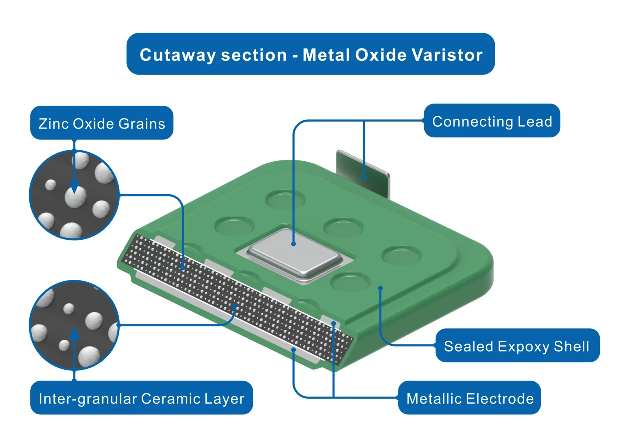
Figure 1: MOV cutaway section showing zinc oxide (ZnO) grains embedded in ceramic matrix with inter-granular boundaries (magnified inset). Each grain boundary forms a microscopic Schottky barrier, creating millions of micro-junctions in series-parallel configuration. The disk’s physical dimensions—thickness determines voltage rating (more boundaries in series), diameter determines current capability (more parallel paths)—directly control surge protection performance.
GDT (Gas Discharge Tube): Structure and Operating Principle
The Gas Discharge Tube takes a fundamentally different approach: instead of clamping voltage with nonlinear resistance, it creates a temporary short circuit when voltage exceeds a threshold. This “crowbar” action diverts surge current through ionized gas rather than solid-state materials.
내부 구조
A GDT consists of two or three electrodes sealed inside a ceramic or glass envelope filled with inert gas (typically a mixture of argon, neon, or xenon at sub-atmospheric pressure). The electrode gap and gas composition determine the breakdown voltage. The hermetic seal is critical—any contamination or pressure change would alter breakdown characteristics.
Three-electrode GDTs are common in telecom applications, providing line-to-line and line-to-ground protection in a single component. Two-electrode versions serve simpler line-to-ground configurations. The electrodes are often coated with materials that reduce the breakdown voltage and stabilize arc formation.
운영 원칙
Under normal conditions, the gas is non-conductive and the GDT presents near-infinite impedance (>10⁹ Ω) with extremely low capacitance—typically below 2 picofarads. When a transient voltage exceeds the spark-over voltage, the electric field ionizes the gas. Free electrons accelerate and collide with gas atoms, liberating more electrons in an avalanche process. Within a fraction of a microsecond, a conductive plasma channel forms between electrodes.
Once ionized, the GDT enters arc mode. Voltage across the device collapses to a low arc voltage—typically 10-20 volts regardless of the initial breakdown voltage. The device now acts as a near-short, diverting surge current through the plasma. The arc persists until current drops below the “glow-to-arc transition current,” typically tens of milliamperes.
This crowbar behavior creates a critical design consideration: if the protected circuit can source sufficient “follow current” above the glow threshold, the GDT may latch in conduction even after the transient ends. This is why GDTs on AC mains require series resistance or coordination with upstream breakers. On low-impedance DC supplies, follow-current latching can be catastrophic.
주요 사양 및 동작
Surge Current Capability: GDTs handle extremely high surge currents—typical telecom-grade devices are rated for 10,000 to 20,000 amperes (8/20 µs waveform) with multi-shot endurance. This high capacity comes from the distributed nature of the plasma channel rather than localized solid-state junctions.
Capacitance: The defining advantage of GDTs is their sub-2 pF capacitance, making them transparent to high-speed signals. This is why they dominate telecom line protection: xDSL, cable broadband, and Gigabit Ethernet can’t tolerate the capacitance of MOVs or many TVS devices.
응답 시간: GDTs are slower than solid-state devices. Breakdown typically occurs within hundreds of nanoseconds to a few microseconds, depending on the voltage overshoot (higher dV/dt accelerates ionization). For fast transients on sensitive electronics, GDTs are often paired with faster clamps in a coordinated protection scheme.
Stability and Lifespan: Quality GDTs exhibit excellent long-term stability. ITU-T K.12 and IEEE C62.31 test methods verify performance over thousands of surge cycles. UL-recognized telecom GDTs demonstrate minimal parameter shift over decades of service.
일반적인 애플리케이션: Telecom line protection (xDSL, cable, fiber optics), high-speed Ethernet interfaces, RF and antenna inputs, and any application where minimal line loading is essential and the surge source impedance is high enough to prevent follow-current latching.
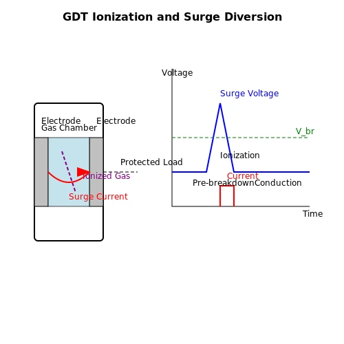
Figure 2: Gas Discharge Tube (GDT) construction and operating behavior. Left diagram shows internal structure: hermetically sealed gas chamber with electrode gap and inert gas fill (argon/neon). Right graph illustrates ionization response—when transient voltage exceeds spark-over threshold, gas ionizes creating conductive plasma channel, voltage collapses to arc mode (~10-20V), and surge current diverts through the plasma until current drops below glow-to-arc transition threshold.
TVS Diode: Structure and Operating Principle
Transient Voltage Suppressor diodes are silicon avalanche devices engineered specifically for surge clamping. They combine the fastest response times with the lowest clamping voltages available in surge protection components, making them the preferred choice for protecting sensitive semiconductor circuits.
내부 구조
A TVS diode is essentially a specialized Zener diode optimized for high pulse power rather than voltage regulation. The silicon die features a heavily doped P-N junction designed to enter avalanche breakdown at a precise voltage. Die area is much larger than equivalent Zener regulators to handle the peak currents of surge events—hundreds of amperes in submicrosecond pulses.
운영 원칙
Under normal operating voltage, the TVS diode operates in reverse bias with only nanoampere-level leakage. When a transient exceeds the reverse breakdown voltage (V_BR), the silicon junction enters avalanche multiplication. Impact ionization generates a flood of electron-hole pairs, and junction resistance collapses. The device clamps voltage at the breakdown level plus the dynamic resistance times the surge current.
The physics is purely solid-state with no mechanical motion, gas ionization, or material phase change. This enables response times in the nanosecond range—sub-1 ns for the bare silicon, though package inductance typically pushes effective response to 1-5 ns for practical devices. The voltage-current characteristic is very steep (low dynamic resistance), providing tight clamping.
주요 사양 및 동작
Pulse Power Ratings: TVS manufacturers specify power capacity using standardized pulse widths (typically 10/1000 µs exponential waveforms). Common product families offer 400W, 600W, 1500W, or 5000W pulse ratings. Peak current capability is calculated from pulse power and clamping voltage—a 600W device with 15V clamp handles about 40A peak.
Clamping Performance: TVS diodes offer the lowest clamping voltages of any surge protection technology. The ratio of clamping voltage to standoff voltage (V_C/V_WM) is typically 1.3 to 1.5, compared to 2.0-2.5 for MOVs. This tight control is critical for protecting 3.3V logic, 5V USB, 12V automotive circuits, and other voltage-sensitive loads.
Capacitance: TVS capacitance varies widely with device construction. Standard junction TVS diodes can exhibit hundreds of picofarads, which loads high-speed data lines. Low-capacitance TVS families engineered for HDMI, USB 3.0, Ethernet, and RF use specialized junction geometries and achieve sub-5 pF per line.
Aging and Reliability: Unlike MOVs, TVS diodes exhibit minimal performance drift under rated pulse stress. The silicon junction doesn’t degrade cumulatively from repeated surges within ratings. Failure modes are typically open-circuit (junction annihilation) or short-circuit (metallization fusing), both of which occur only under extreme overload well beyond ratings.
일반적인 애플리케이션: Board-level circuit protection (I/O ports, power rails), USB and HDMI interfaces, automotive electronics, DC power supplies, communication data lines, and any application requiring fast response and tight voltage clamping for semiconductor loads.
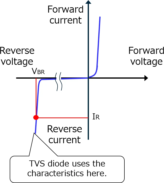
Figure 3: TVS diode voltage-current (I-V) characteristic curve showing semiconductor avalanche operation. Under normal voltage (V_WM standoff region), device maintains high impedance with nanoampere leakage. When transient exceeds reverse breakdown voltage (V_BR), silicon P-N junction enters avalanche multiplication—junction resistance collapses and device clamps voltage at V_C (breakdown voltage plus dynamic resistance × surge current). The steep curve (low dynamic resistance) provides tight voltage control critical for protecting semiconductor loads.
Clamping vs Crowbar: Two Protection Philosophies
The fundamental difference between these technologies lies in their protection philosophy. MOVs and TVS diodes are clamping devices—they limit voltage to a specific level proportional to surge current. GDTs are crowbar devices—they create a short circuit that collapses voltage to a low residual level regardless of current magnitude.
Clamping behavior (MOV and TVS): As surge current increases, clamping voltage rises according to the device’s nonlinear V-I curve. A MOV rated 275V RMS might clamp at 750V for a 1 kA surge but rise to 900V at 5 kA. A TVS diode rated 15V standoff might clamp at 24V for 10A but reach 26V at 20A. The protected load sees a voltage determined by surge amplitude and device characteristics.
Crowbar behavior (GDT): Once breakdown occurs, the GDT enters arc mode and voltage collapses to 10-20V regardless of whether surge current is 100A or 10,000A. This provides excellent protection once triggered, but the initial spark-over can allow a voltage spike before ionization completes. This is why sensitive loads behind GDTs often need a secondary fast clamp.
Each philosophy suits different applications. Clamping devices protect by limiting voltage exposure. Crowbar devices protect by diverting current. Clamping works when the protected circuit can tolerate the clamp voltage. Crowbar works when the surge source has high enough impedance that shorting the line doesn’t damage upstream equipment or cause follow-current problems.
MOV vs GDT vs TVS: Side-by-Side Comparison
The table below quantifies the key performance differences across these three surge protection technologies:
| 매개변수 | MOV (Metal Oxide Varistor) | GDT (Gas Discharge Tube) | TVS 다이오드 |
| 운영 원칙 | Voltage-dependent nonlinear resistance (ZnO grain boundaries) | Gas ionization crowbar | Semiconductor avalanche breakdown |
| 보호 메커니즘 | Clamping | Crowbar | Clamping |
| 응답 시간 | <25 ns (typical catalog parts) | 100 ns – 1 µs (voltage-dependent) | 1-5 ns (package-limited) |
| Clamping/Arc Voltage | 2.0-2.5 × MCOV | 10-20 V (arc mode) | 1.3-1.5 × V_standoff |
| Surge Current (8/20 µs) | 400 A – 100 kA (size-dependent) | 5 kA – 20 kA (telecom-grade) | 10 A – 200 A (600W family ~40A) |
| 에너지 처리량 | Excellent (100-1000 J) | Excellent (distributed plasma) | Moderate (limited by junction) |
| Capacitance | 50-5000 pF (area-dependent) | <2 pF | 5-500 pF (construction-dependent) |
| Aging Behavior | Degrades with surge cycles; V_n drifts down | Stable over thousands of surges | Minimal drift within ratings |
| Failure Mode | Degradation → short or open | Short (arc sustaining) | Open or short (catastrophic only) |
| Follow-Current Risk | Low (self-extinguishing) | High (requires external limiting) | None (solid-state) |
| Typical Voltage Range | 18V RMS – 1000V RMS | 75V – 5000V DC sparkover | 3.3V – 600V standoff |
| Cost (Relative) | Low ($0.10 – $5) | Low-Medium ($0.50 – $10) | Low-Medium ($0.20 – $8) |
| 표준 | IEC 61643-11, UL 1449 | ITU-T K.12, IEEE C62.31 | IEC 61643-11, UL 1449 |
| 주요 애플리케이션 | AC mains, power distribution, industrial | Telecom lines, high-speed data, antenna | Board-level I/O, DC supplies, automotive |
Key Takeaways from the Comparison
영화 offer the best balance of energy handling, fast response, and cost for power-level surges. They dominate AC mains protection but suffer from capacitance loading on high-frequency circuits and cumulative aging under repeated stress.
GDTs excel where minimal line loading is critical and surge current capability must be maximized. Their ultra-low capacitance makes them irreplaceable in telecom and RF applications, but slower response and follow-current risk require careful circuit design.
TVS diodes provide the fastest, tightest clamping for sensitive electronics. They are the only practical choice for protecting semiconductor I/O at voltages below 50V, but limited energy capacity means they can’t handle the lightning-level surges that MOVs and GDTs routinely absorb.
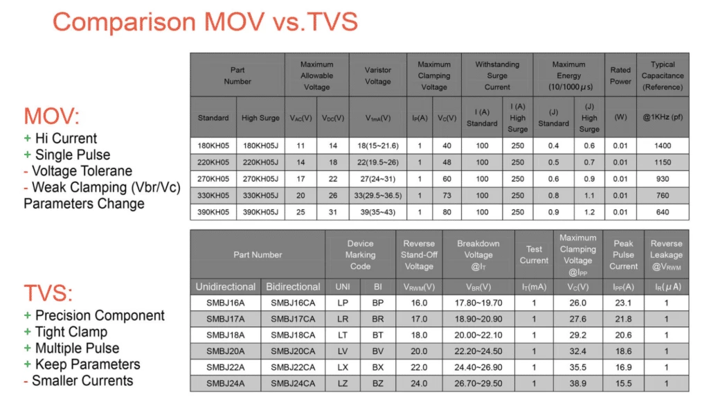
그림 4: 주요 사양에 따른 MOV(금속 산화물 배리스터) 및 TVS(과도 전압 억제기) 기술을 대조하는 전문가 비교 차트입니다. MOV는 전력 수준 서지에 대한 탁월한 에너지 흡수와 함께 더 높은 클램핑 전압 비율(2.0-2.5× MCOV)을 나타내는 반면, TVS 다이오드는 반도체 보호를 위해 더 빠른 응답(<5ns)으로 더 엄격한 전압 제어(1.3-1.5× 스탠드오프)를 제공합니다. 이 표에는 전압 정격, 서지 전류 기능 및 각 기술의 보완적인 성능 범위를 보여주는 일반적인 부품 번호 예가 포함되어 있습니다.
기술 선택 가이드: 각 기술을 사용하는 시기
올바른 서지 보호 기술을 선택하는 것은 장치 특성을 회로 요구 사항에 맞추는 데 달려 있습니다. 다음은 의사 결정 프레임워크입니다.
MOV 사용 시기:
- 회로 전압이 AC 주전원 또는 고전압 DC(>50V)인 경우MOV는 18V RMS에서 1000V 이상까지의 전압 정격으로 제공되어 주거용(120/240V), 상업용(277/480V) 및 산업용 전력 분배에 완벽하게 부합합니다.
- 서지 에너지가 높은 경우낙뢰로 인한 서지, 유틸리티 스위칭 과도 현상 및 모터 돌입은 MOV만이 경제적으로 흡수할 수 있는 에너지 수준(수백에서 수천 줄)을 생성합니다.
- 응답 시간 <25ns가 허용되는 경우대부분의 전력 전자 장치 및 산업 장비는 MOV 응답 속도를 허용합니다.
- 정전 용량 로딩이 허용되는 경우전력 주파수(50/60Hz)에서 1000pF 정전 용량도 무시할 수 있습니다.
- 비용이 제한적인 경우MOV는 줄당 가장 낮은 보호 비용을 제공합니다.
다음과 같은 경우 MOV를 피하십시오. 고속 통신 회선(정전 용량 로딩), 저전압 반도체 회로(클램핑 전압이 너무 높음) 또는 수십 년 동안 보장된 드리프트 없는 성능이 필요한 애플리케이션(노화 문제)을 보호합니다.
GDT 사용 시기:
- 라인 로딩이 최소화되어야 하는 경우(<2pF)xDSL 모뎀, 케이블 광대역, 기가비트 이더넷, RF 수신기 및 안테나 입력은 MOV 또는 표준 TVS 장치의 정전 용량을 허용할 수 없습니다.
- 서지 전류 기능이 최대화되어야 하는 경우통신 중앙 사무실, 셀 타워 및 실외 설치는 TVS 정격을 초과하는 반복적인 고진폭 낙뢰 서지에 직면합니다.
- 보호된 회로의 소스 임피던스가 높은 경우전화선(600Ω), 안테나 피드라인(50-75Ω) 및 데이터 케이블은 과도한 후속 전류 없이 안전하게 단락될 수 있습니다.
- 작동 전압이 높은 경우(>100V)GDT는 75V에서 5000V까지의 스파크오버 전압으로 제공되어 통신 전압, PoE(Power over Ethernet) 및 고전압 신호 처리를 포괄합니다.
다음과 같은 경우 GDT를 피하십시오. 저임피던스 DC 전원 공급 장치(후속 전류 위험), 가장 빠른 응답이 필요한 회로(<100ns 중요) 또는 초기 스파크오버 스파이크를 허용할 수 없는 전압에 민감한 부하(보조 클램핑 필요)를 보호합니다.
TVS 다이오드 사용 시기:
- 클램핑 전압을 엄격하게 제어해야 하는 경우3.3V 로직, 5V USB, 12V 자동차 회로 및 기타 반도체 부하는 공칭 전압의 20-30% 이내로 클램핑해야 합니다. TVS 다이오드만이 이를 제공합니다.
- 응답 시간이 가장 빨라야 하는 경우(<5ns)고속 프로세서, FPGA 및 민감한 아날로그 회로를 보호하려면 나노초 응답이 필요합니다.
- 회로 전압이 낮음에서 중간(<100V)인 경우TVS 제품군은 3.3V 데이터 라인에서 48V 통신 전원 공급 장치까지 모든 것을 포괄합니다.
- 노화/드리프트를 허용할 수 없는 경우의료 기기, 항공 우주 및 안전에 중요한 시스템은 제품 수명 동안 예측 가능하고 안정적인 보호가 필요합니다.
- 보드 공간이 제한적인 경우0402 또는 SOT-23 패키지의 SMT TVS 장치는 MOV 및 GDT가 들어갈 수 없는 곳에 적합합니다.
다음과 같은 경우 TVS 다이오드를 피하십시오. 서지 에너지가 펄스 전력 정격을 초과하는 경우(일반적인 600W 장치는 ~1줄만 흡수), 서지 전류가 피크 정격을 초과하는 경우(15V에서 600W의 경우 일반적인 40A) 또는 다중 라인 시스템에서 채널당 비용이 너무 비싸지는 경우.
의사 결정 매트릭스
| 응용 프로그램 | 기본 기술 | 이론적 해석 |
| AC 주전원 패널 보호 | MOV(유형 1/2 SPD) | 고에너지, 120-480V, 비용 효율적 |
| 통신 회선 인터페이스 | GDT + TVS(단계별) | GDT는 에너지를 흡수하고 TVS는 잔류물을 클램프합니다. |
| USB 2.0 / 3.0 데이터 라인 | 저용량 TVS | 빠른 에지, 5V 전원 공급 장치, <5pF 필요 |
| 이더넷(10/100/1000 Base-T) | GDT(기본) + 저용량 TVS | 최소 로딩, 높은 서지 노출 |
| 24V DC 산업 I/O | TVS | 강력한 클램프, 빠른 응답, 노화 없음 |
| PV 태양광 DC 입력 | MOV(DC 정격) | 고전압(600-1000V), 고에너지 |
| 자동차 12V 회로 | TVS | 로드 덤프 보호, 24-36V에서 강력한 클램프 |
| RF 안테나 입력 | GDT | 2pF 미만, 높은 전력 처리 |
| 3.3V FPGA 전원 레일 | TVS(저용량) | 6-8V 클램프, <1ns 응답이 중요함 |
이 매트릭스는 시작점입니다. 복잡한 설치는 종종 계층화된 보호 체계에서 기술을 결합하여 각 단계의 강점을 활용합니다.
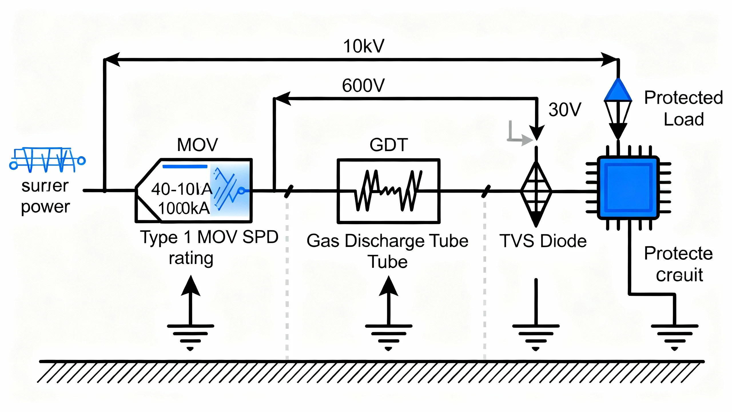
그림 5: 조정된 보호 전략을 보여주는 전문적인 3단계 서지 보호 아키텍처 다이어그램. 1단계(기본): 서비스 입구의 1형 MOV SPD는 극심한 서지 에너지(40-100kA)를 처리하고 전압을 10+kV에서 ~600V로 클램프합니다. 2단계(보조): 가스 방전 튜브는 잔류 고전압 과도 현상을 전환하고 아크 모드 작동을 통해 전압을 ~30V로 줄입니다. 3단계(최종): TVS 다이오드는 민감한 반도체 부하를 보호하기 위해 나노초 응답으로 강력한 클램핑(<1.5× 스탠드오프 전압)을 제공합니다. 각 단계는 업스트림 장치가 다운스트림 구성 요소보다 먼저 트리거되도록 적절한 접지 및 전압 조정을 특징으로 하여 보호 캐스케이드 전체에 서지 에너지를 분산시키는 명확한 “핸드오프” 지점을 만듭니다. 이 계층화된 접근 방식은 MOV(고에너지), GDT(저용량) 및 TVS(강력한 클램프) 기술의 상호 보완적인 강점을 활용합니다.
계층화된 보호: 기술 결합
가장 강력한 서지 보호 아키텍처는 단일 기술에 의존하지 않습니다. 대신 위협 스펙트럼의 서로 다른 부분에 최적화된 여러 단계를 조정합니다. 이 “심층 방어” 접근 방식은 MOV, GDT 및 TVS 기술의 상호 보완적인 강점을 활용합니다.
계층 보호가 필요한 이유?
에너지 분배: 단일 TVS 다이오드는 10kA 낙뢰 서지를 흡수할 수 없지만 업스트림 GDT는 해당 에너지의 99%를 전환하여 TVS가 잔류물을 클램프하도록 할 수 있습니다. 각 단계는 가장 잘하는 것을 처리합니다.
속도 최적화: GDT가 이온화되는 데 수백 나노초가 걸립니다. 그 동안 빠른 TVS 다운스트림은 초기 스파이크를 클램프하여 민감한 부하의 손상을 방지할 수 있습니다. GDT가 작동되면 벌크 전류 전환을 인계합니다.
전압 조정: 업스트림 장치는 다운스트림 장치보다 먼저 고장나야 합니다. 적절한 선택을 통해 첫 번째 단계가 예를 들어 600V에서 전도되어 두 번째 단계(정격 150V)에 도달하는 것을 제한하고, 이는 최종 부하(정격 50V)를 보호합니다.
일반적인 계층화된 아키텍처
통신 인터페이스(GDT + TVS):
- 기본 단계: 인터페이스 경계의 GDT는 직접적인 낙뢰 및 고전압 전원 오류(2-10kV 서지, 최대 20kA)를 처리합니다.
- 보조 단계: 저용량 TVS 다이오드는 트랜시버 IC(<30V)에 대한 안전한 수준으로 잔류 과도 현상을 클램프합니다.
- 조정GDT 스파크오버 400V, TVS 항복 15V, 트랜시버 최대 정격 12V. TVS는 GDT 이온화 지연 중에 보호합니다. GDT가 작동되면 벌크 전류 의무를 가정합니다.
이더넷 PoE(GDT + TVS + 인덕터):
- 기본GDT는 라인-접지 낙뢰 서지를 전환합니다.
- 직렬 인덕터: 서지 상승 시간(dV/dt)을 늦추어 GDT가 이온화될 시간을 주고 다운스트림 단계로의 전류를 제한합니다.
- 보조각 차동 쌍의 TVS 다이오드는 공통 모드 및 차동 모드 과도 현상을 클램프하여 이더넷 PHY(최대 ±8V)를 보호합니다.
산업용 AC 패널(MOV 기본 + MOV 보조):
- 서비스 입구1형 MOV 정격 40-100kA는 직접적인 낙뢰를 처리합니다(IEC 61643-11에 따른 1.2/50µs 전압, 10/350µs 전류 파형).
- 배전반2형 MOV 정격 20-40kA는 건물 배선을 통해 결합되는 잔류 서지를 클램프합니다.
- 부하 장비3형 SPD 또는 보드 수준 TVS는 최종 사용 지점 보호를 제공합니다.
PV 태양광 시스템(MOV DC + TVS):
- 어레이 정션 박스PV 스트링 출력의 DC 정격 MOV(600-1000V)는 낙뢰로 인한 서지를 처리합니다.
- 인버터 입력: TVS 다이오드는 DC-DC 컨버터 및 MPPT 컨트롤러 반도체를 보호하며, 실리콘이 견딜 수 있는 수준으로 클램핑합니다.
성공적인 조정을 위한 핵심은 명확한 “핸드오프” 지점을 만드는 항복 전압을 선택하고 한 단계에서 나오는 에너지가 다음 단계의 정격 내에 유지되는지 확인하는 것입니다. VIOX와 같은 완전한 SPD 시스템 제조업체는 종종 이러한 설계 복잡성을 제거하는 테스트를 거친 조정된 어셈블리를 게시합니다.
결론
서지 보호 구성 요소를 선택하는 것은 “최고'의 기술을 찾는 것이 아니라 물리학을 요구 사항에 맞추는 것입니다. MOV는 산화 아연 세라믹을 활용하여 전력 전압에서 높은 에너지를 흡수합니다. GDT는 가스 이온화를 활용하여 최대 전류 용량으로 최소한의 라인 로딩을 달성합니다. TVS 다이오드는 반도체 애벌랜치를 활용하여 민감한 전자 장치를 가장 빠르고 가장 강력하게 클램핑합니다.
각 기술은 근본적인 절충점을 나타냅니다.
- MOV는 더 높은 클램핑 전압과 노화를 감수하는 대신 뛰어난 에너지 처리 능력과 비용을 제공합니다.
- GDT는 느린 응답과 후속 전류 위험을 감수하는 대신 초저 정전 용량과 서지 내구성을 제공합니다.
- TVS 다이오드는 제한된 에너지 용량을 감수하는 대신 가장 빠른 응답과 가장 강력한 전압 제어를 제공합니다.
우리가 살펴본 작동 원리에 뿌리를 둔 이러한 절충점을 이해하면 실제로 애플리케이션에서 작동하는 보호 기능을 지정할 수 있습니다. 5V 데이터 라인에 있는 600V MOV는 보호에 실패합니다. 10kA 낙뢰 서지에 직면한 40A TVS 다이오드는 치명적으로 고장납니다. 낮은 임피던스 DC 전원 공급 장치에 있는 GDT는 파괴적인 후속 전류 전도로 래치될 수 있습니다.
복잡한 설치의 경우 계층화된 보호 기능은 여러 기술을 조정하여 각 기술이 가장 잘 수행되는 위치에 배치합니다. GDT는 벌크 에너지를 흡수하고, MOV는 전력 수준 서지를 처리하고, TVS는 반도체 부하에 대한 최종 단계 클램핑을 제공합니다.
IEC 61643-11에 따라 100kA로 정격된 전력 분배 SPD를 설계하든, 2pF 미만의 로딩으로 기가비트 이더넷 인터페이스를 보호하든, 3.3V FPGA I/O를 보호하든, 의사 결정 프레임워크는 동일합니다. 장치 물리학을 회로 요구 사항에 맞추고, 위협 파형에 대한 정격을 확인하고, 단일 기술로 전체 스펙트럼을 포괄할 수 없는 경우 단계를 조정합니다.
복스 일렉트릭 소개: 서지 보호 장치 제조업체인 VIOX는 주거, 상업 및 산업 애플리케이션을 위한 포괄적인 MOV, GDT 및 TVS 솔루션을 제공합니다. 당사의 엔지니어링 팀은 조정된 보호 시스템에 대한 애플리케이션 지원을 제공합니다. 방문 www.viox.com 또는 사양 지원을 위해 기술 영업 팀에 문의하십시오.