ແນະນຳ
在为电气系统指定浪涌保护方案时,工程师面临三种核心技术的根本性选择:金属氧化物压敏电阻(MOV)、气体放电管(GDT)和瞬态电压抑制(TVS)二极管。每种技术基于不同的物理原理提供独特的性能特征——MOV利用非线性陶瓷电阻特性,GDT依赖气体电离效应,TVS二极管则运用半导体雪崩击穿原理。.
技术选择并非寻找“最优”方案,而是根据应用需求匹配根本性的性能权衡。在交流配电系统中表现出色的MOV,若用于高速数据线路可能导致灾难性故障;适用于电信接口的GDT若部署在5V直流电源轨上则完全错误;为板级I/O设计的TVS二极管在暴露于雷电的户外电路中可能不堪重负。.
本文将从基本原理出发剖析每种技术,阐释其性能差异背后的物理机制,并在响应时间、钳位电压、能量耐受、电容特性、老化行为和成本等方面提供量化对比。无论您是设计配电系统 SPD, 、保护通信接口,还是协调多级保护方案,理解这些根本差异将帮助您选择真正具备保护功能的元件——而非仅仅满足采购清单要求。.
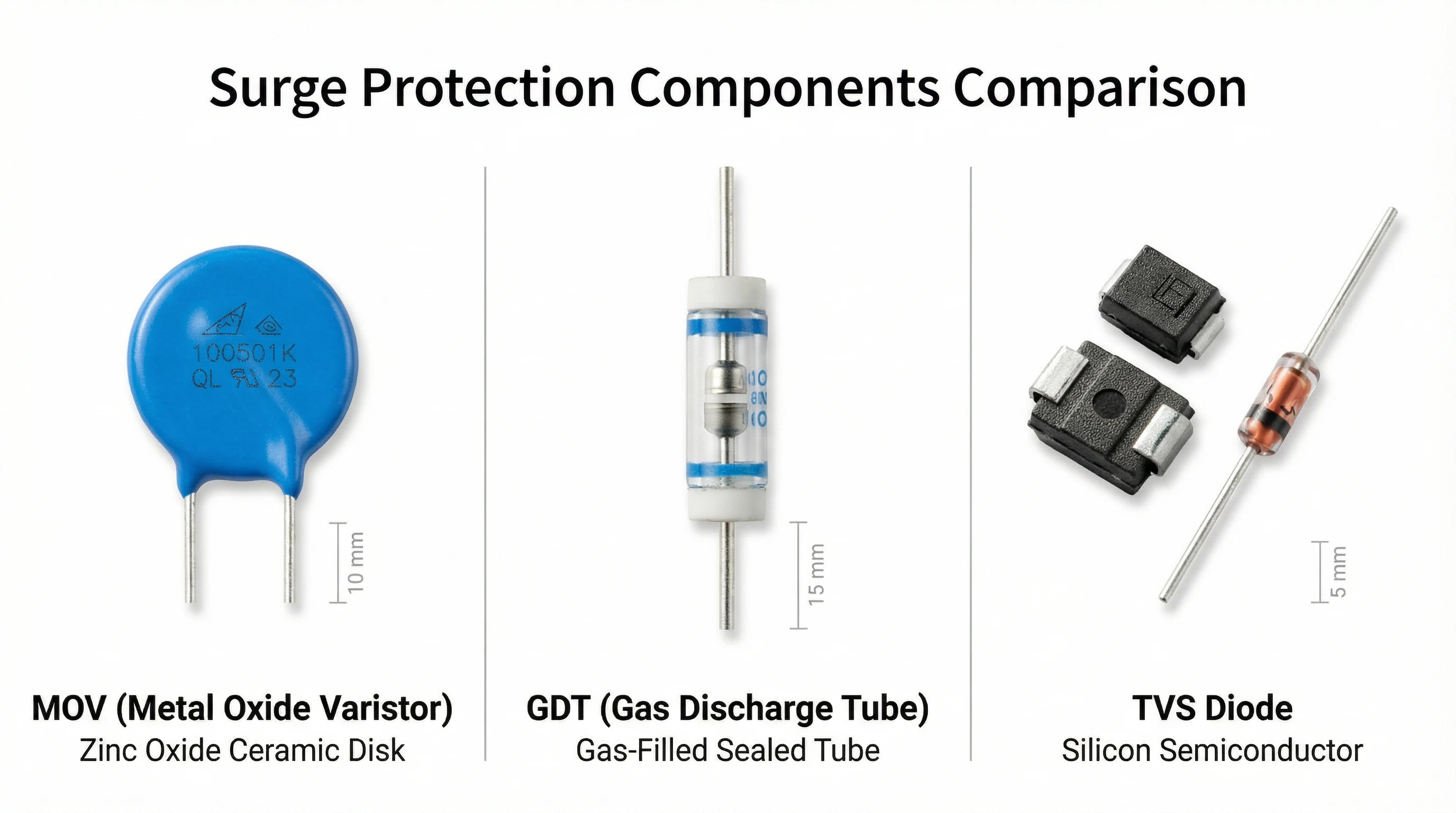
图0:三种浪涌保护技术的物理结构对比。左:MOV(金属氧化物压敏电阻)呈现典型的蓝色氧化锌陶瓷圆盘与径向引线结构——物理尺寸随额定电压(圆盘厚度)和通流容量(圆盘直径)按比例变化。中:GDT(气体放电管)展示圆柱形密封玻璃/陶瓷外壳,内含惰性气体与电极——气密结构确保稳定的火花放电特性。右:TVS二极管展示从紧凑型贴片封装(0402、SOT-23)到较大通孔封装(DO-201、DO-218)等多种半导体封装形式——硅片尺寸决定脉冲功率额定值。这些显著的物理差异反映了根本不同的工作原理:陶瓷晶界结(MOV)、气体电离等离子体(GDT)和半导体雪崩击穿(TVS)。.
MOV(金属氧化物压敏电阻):结构与工作原理
金属氧化物压敏电阻是一种陶瓷半导体器件,其电阻值随电压升高急剧下降。这种压敏特性使其如同自动电压钳位器——在浪涌期间大电流导通,在正常运行时几乎隐形。.
内部结构
MOV由氧化锌(ZnO)晶粒与微量铋、钴、锰等金属氧化物烧结而成。其奥秘在于晶界处:相邻ZnO晶粒间的每个边界都形成微观肖特基势垒——本质上是一对背靠背的微型二极管结。单个MOV圆盘包含数百万个这样的微结,以复杂的三维串并联网络连接。.
器件的整体特性源于这种微观结构。圆盘厚度决定工作电压(串联晶界数量越多,额定电压越高);圆盘直径决定通流能力(并联路径越多,浪涌电流容量越大)。因此MOV数据手册会标注每毫米厚度的压敏电压值,而配电系统用高能MOV通常采用物理尺寸较大的块状或圆盘组件。.
ຫຼັກການປະຕິບັດງານ
当电压低于压敏电压(Vᵥ)时,晶界结保持耗尽状态,器件仅吸收微安级漏电流。当浪涌电压超过Vᵥ时,结区通过量子隧穿和雪崩倍增效应击穿,电阻从兆欧级骤降至欧姆级,MOV将浪涌电流泄放至地。.
这种转变本质上是快速的——材料层面的响应可达亚纳秒级。标准目录MOV的响应时间低于25纳秒,主要受引线电感和封装结构限制,而非ZnO物理特性制约。其电压-电流特性呈现高度非线性,通常用公式I = K·Vᵅ描述,非线性系数α范围为25至50(线性电阻的α=1)。.
关键参数与特性
能量耐受:MOV在吸收浪涌能量方面表现卓越。制造商采用2毫秒矩形脉冲标定能量容量,使用标准8/20微秒波形标定浪涌电流。配电用块状MOV单次事件可处理10,000至100,000安培浪涌电流。.
老化与退化:反复承受浪涌会导致累积性微观结构损伤。压敏电压逐渐下降,漏电流增加,钳位性能退化。严重过载可能击穿晶界,形成永久性导电路径。因此数据手册会规定重复浪涌的降额系数,关键安装场景应将MOV漏电流作为维护参数进行监测。.
ຄໍາຮ້ອງສະຫມັກທົ່ວໄປ: ການປ້ອງກັນໄຟກະຊາກ AC, ກະດານແຈກຢາຍໄຟຟ້າ, ໄດຣຟມໍເຕີອຸດສາຫະກໍາ, ອຸປະກອນໜັກ, ແລະ ການນໍາໃຊ້ໃດໆທີ່ຕ້ອງການການດູດຊຶມພະລັງງານສູງ ດ້ວຍການຕອບສະໜອງໄວ (ນາໂນວິນາທີ).
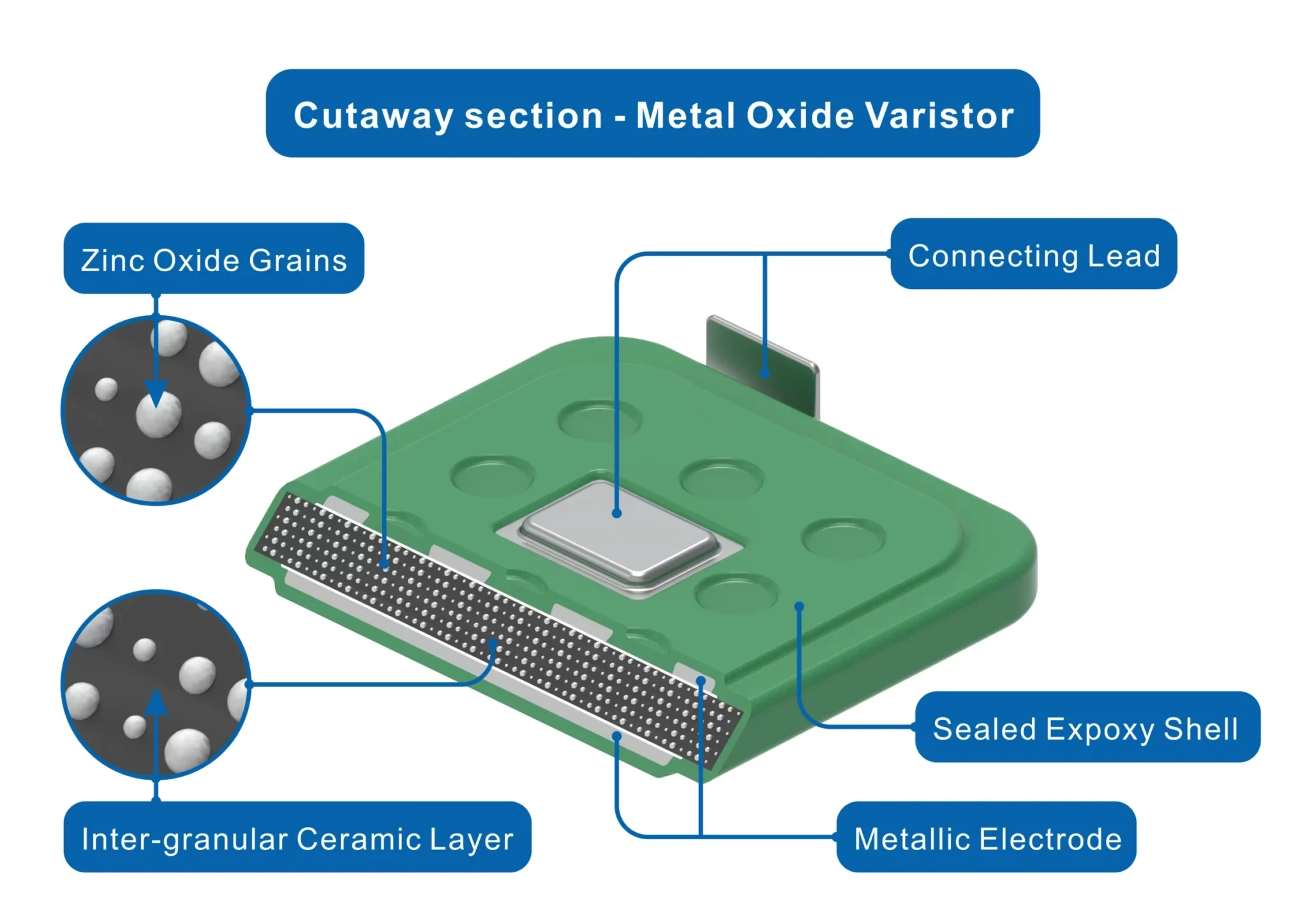
ຮູບທີ 1: ພາກສ່ວນຕັດ MOV ສະແດງໃຫ້ເຫັນເມັດສັງກະສີອອກໄຊ (ZnO) ທີ່ຝັງຢູ່ໃນເມຕຣິກເຊລາມິກ ທີ່ມີຂອບເຂດລະຫວ່າງເມັດ (ຂະຫຍາຍໃຫຍ່). ແຕ່ລະຂອບເຂດເມັດສ້າງເປັນສິ່ງກີດຂວາງ Schottky ຈຸລະພາກ, ສ້າງຈຸດເຊື່ອມຕໍ່ຈຸລະພາກຫຼາຍລ້ານຈຸດໃນການຕັ້ງຄ່າຂະໜານຊຸດ. ຂະໜາດທາງກາຍະພາບຂອງແຜ່ນ—ຄວາມໜາເປັນຕົວ ກຳນົດລະດັບແຮງດັນ (ຂອບເຂດຫຼາຍກວ່າໃນຊຸດ), ເສັ້ນຜ່າສູນກາງເປັນຕົວ ກຳນົດຄວາມສາມາດໃນການຮັບກະແສ (ເສັ້ນທາງຂະໜານຫຼາຍກວ່າ)—ຄວບຄຸມປະສິດທິພາບການປ້ອງກັນໄຟກະຊາກໂດຍກົງ.
GDT (ທໍ່ລະບາຍອາຍແກັສ): ໂຄງສ້າງ ແລະ ຫຼັກການເຮັດວຽກ
ທໍ່ລະບາຍອາຍແກັສໃຊ້ວິທີການທີ່ແຕກຕ່າງກັນໂດຍພື້ນຖານ: ແທນທີ່ຈະຈໍາກັດແຮງດັນດ້ວຍຄວາມຕ້ານທານທີ່ບໍ່ເປັນເສັ້ນຊື່, ມັນສ້າງວົງຈອນສັ້ນຊົ່ວຄາວເມື່ອແຮງດັນເກີນຂອບເຂດ. ການກະທໍາ “crowbar” ນີ້ປ່ຽນທິດທາງກະແສໄຟກະຊາກຜ່ານອາຍແກັສທີ່ແຕກຕົວເປັນໄອອອນແທນທີ່ຈະເປັນວັດສະດຸຂອງແຂງ.
内部结构
GDT ປະກອບດ້ວຍສອງຫຼືສາມເອເລັກໂຕຣດທີ່ຜະນຶກເຂົ້າກັນພາຍໃນຊອງເຊລາມິກຫຼືແກ້ວທີ່ເຕັມໄປດ້ວຍອາຍແກັສທີ່ບໍ່ມີປະຕິກິລິຍາ (ໂດຍປົກກະຕິແມ່ນສ່ວນປະສົມຂອງ argon, neon, ຫຼື xenon ຢູ່ຄວາມກົດດັນຕໍ່າກວ່າບັນຍາກາດ). ຊ່ອງຫວ່າງຂອງເອເລັກໂຕຣດ ແລະ ອົງປະກອບຂອງອາຍແກັສເປັນຕົວ ກຳນົດແຮງດັນໄຟຟ້າແຮງສູງ. ການຜະນຶກແໜ້ນແມ່ນມີຄວາມສໍາຄັນ—ການປົນເປື້ອນ ຫຼື ການປ່ຽນແປງຄວາມກົດດັນໃດໆກໍຈະປ່ຽນແປງຄຸນລັກສະນະການແຮງດັນໄຟຟ້າແຮງສູງ.
GDT ສາມເອເລັກໂຕຣດແມ່ນພົບເລື້ອຍໃນການນໍາໃຊ້ໂທລະຄົມ, ໃຫ້ການປ້ອງກັນສາຍຕໍ່ສາຍ ແລະ ສາຍຕໍ່ດິນໃນອົງປະກອບດຽວ. ຮຸ່ນສອງເອເລັກໂຕຣດໃຫ້ບໍລິການການຕັ້ງຄ່າສາຍຕໍ່ດິນທີ່ງ່າຍກວ່າ. ເອເລັກໂຕຣດມັກຈະຖືກເຄືອບດ້ວຍວັດສະດຸທີ່ຊ່ວຍຫຼຸດຜ່ອນແຮງດັນໄຟຟ້າແຮງສູງ ແລະ ສະຖຽນລະພາບການສ້າງ arc.
ຫຼັກການປະຕິບັດງານ
ພາຍໃຕ້ສະພາບປົກກະຕິ, ອາຍແກັສບໍ່ນໍາໄຟຟ້າ ແລະ GDT ສະແດງຄວາມຕ້ານທານທີ່ໃກ້ຈະບໍ່ມີຂອບເຂດ (>10⁹ Ω) ດ້ວຍຄວາມຈຸຕໍ່າຫຼາຍ—ໂດຍປົກກະຕິແມ່ນຕໍ່າກວ່າ 2 picofarads. ເມື່ອແຮງດັນຊົ່ວຄາວເກີນແຮງດັນໄຟຟ້າແຮງສູງ, ສະໜາມໄຟຟ້າຈະເຮັດໃຫ້ອາຍແກັສແຕກຕົວເປັນໄອອອນ. ເອເລັກໂຕຣນິກອິດສະລະເລັ່ງ ແລະ ຕຳກັບອະຕອມຂອງອາຍແກັສ, ປົດປ່ອຍເອເລັກໂຕຣນິກຫຼາຍຂຶ້ນໃນຂະບວນການ avalanche. ພາຍໃນສ່ວນໜຶ່ງຂອງໄມໂຄຣວິນາທີ, ຊ່ອງທາງ plasma ທີ່ນໍາໄຟຟ້າໄດ້ສ້າງຂຶ້ນລະຫວ່າງເອເລັກໂຕຣດ.
ເມື່ອແຕກຕົວເປັນໄອອອນແລ້ວ, GDT ຈະເຂົ້າສູ່ໂໝດ arc. ແຮງດັນໄຟຟ້າທົ່ວອຸປະກອນຫຼຸດລົງເປັນແຮງດັນ arc ຕ່ຳ—ໂດຍປົກກະຕິແມ່ນ 10-20 ໂວນ ໂດຍບໍ່ຄໍານຶງເຖິງແຮງດັນໄຟຟ້າແຮງສູງເບື້ອງຕົ້ນ. ດຽວນີ້ອຸປະກອນເຮັດໜ້າທີ່ເປັນວົງຈອນໃກ້ສັ້ນ, ປ່ຽນທິດທາງກະແສໄຟກະຊາກຜ່ານ plasma. arc ຍັງຄົງຢູ່ຈົນກວ່າກະແສໄຟຟ້າຈະຫຼຸດລົງຕໍ່າກວ່າ “ກະແສການປ່ຽນແປງຈາກແສງເປັນ arc,” ໂດຍປົກກະຕິແມ່ນສິບສ່ວນຮ້ອຍຂອງ milliamperes.
ພຶດຕິກໍາ crowbar ນີ້ສ້າງການພິຈາລະນາການອອກແບບທີ່ສໍາຄັນ: ຖ້າວົງຈອນທີ່ຖືກປົກປ້ອງສາມາດສະໜອງ “ກະແສຕິດຕາມ” ທີ່ພຽງພໍສູງກວ່າຂອບເຂດແສງ, GDT ອາດຈະຄ້າງຢູ່ໃນການນໍາໄຟຟ້າເຖິງແມ່ນວ່າຫຼັງຈາກເຫດການຊົ່ວຄາວສິ້ນສຸດລົງ. ນີ້ແມ່ນເຫດຜົນທີ່ວ່າ GDTs ໃນສາຍໄຟ AC ຕ້ອງການຄວາມຕ້ານທານຊຸດ ຫຼື ການປະສານງານກັບຕົວຕັດວົງຈອນຂັ້ນເທິງ. ໃນການສະໜອງ DC ຄວາມຕ້ານທານຕໍ່າ, ການຄ້າງກະແສຕິດຕາມສາມາດເປັນອັນຕະລາຍໄດ້.
关键参数与特性
ຄວາມສາມາດໃນການຮັບກະແສໄຟກະຊາກ: GDTs ສາມາດຮັບກະແສໄຟກະຊາກທີ່ສູງຫຼາຍ—ອຸປະກອນລະດັບໂທລະຄົມປົກກະຕິແມ່ນຖືກຈັດອັນດັບສໍາລັບ 10,000 ຫາ 20,000 ແອມແປ (ຮູບແບບຄື້ນ 8/20 µs) ດ້ວຍຄວາມທົນທານຫຼາຍຄັ້ງ. ຄວາມສາມາດສູງນີ້ມາຈາກລັກສະນະການແຈກຢາຍຂອງຊ່ອງທາງ plasma ແທນທີ່ຈະເປັນຈຸດເຊື່ອມຕໍ່ຂອງແຂງທີ່ຕັ້ງຢູ່.
ຄວາມຈຸ: ຂໍ້ໄດ້ປຽບທີ່ກໍານົດຂອງ GDTs ແມ່ນຄວາມຈຸຕໍ່າກວ່າ 2 pF ຂອງພວກມັນ, ເຮັດໃຫ້ພວກມັນໂປ່ງໃສຕໍ່ສັນຍານຄວາມໄວສູງ. ນີ້ແມ່ນເຫດຜົນທີ່ພວກເຂົາຄອບງໍາການປ້ອງກັນສາຍໂທລະຄົມ: xDSL, ສາຍເຄເບີ້ນບຣອດແບນ, ແລະ Gigabit Ethernet ບໍ່ສາມາດທົນທານຕໍ່ຄວາມຈຸຂອງ MOVs ຫຼືອຸປະກອນ TVS ຈໍານວນຫຼາຍ.
ເວລາຕອບສະຫນອງ: GDTs ຊ້າກວ່າອຸປະກອນຂອງແຂງ. ການແຮງດັນໄຟຟ້າແຮງສູງໂດຍປົກກະຕິເກີດຂຶ້ນພາຍໃນຫຼາຍຮ້ອຍນາໂນວິນາທີ ຫາ ສອງສາມໄມໂຄຣວິນາທີ, ຂຶ້ນກັບແຮງດັນເກີນ (dV/dt ທີ່ສູງກວ່າເລັ່ງການແຕກຕົວເປັນໄອອອນ). ສໍາລັບເຫດການຊົ່ວຄາວທີ່ໄວໃນອຸປະກອນເອເລັກໂຕຣນິກທີ່ລະອຽດອ່ອນ, GDTs ມັກຈະຖືກຈັບຄູ່ກັບຕົວຈໍາກັດທີ່ໄວກວ່າໃນໂຄງການປ້ອງກັນທີ່ປະສານງານກັນ.
ສະຖຽນລະພາບ ແລະ ອາຍຸການໃຊ້ງານ: GDTs ທີ່ມີຄຸນນະພາບສະແດງໃຫ້ເຫັນເຖິງສະຖຽນລະພາບໃນໄລຍະຍາວທີ່ດີເລີດ. ວິທີການທົດສອບ ITU-T K.12 ແລະ IEEE C62.31 ກວດສອບປະສິດທິພາບໃນໄລຍະຫຼາຍພັນຮອບວຽນໄຟກະຊາກ. GDTs ໂທລະຄົມທີ່ໄດ້ຮັບການຮັບຮອງຈາກ UL ສະແດງໃຫ້ເຫັນການປ່ຽນແປງພາລາມິເຕີໜ້ອຍທີ່ສຸດໃນໄລຍະຫຼາຍສິບປີຂອງການບໍລິການ.
ຄໍາຮ້ອງສະຫມັກທົ່ວໄປ: ການປ້ອງກັນສາຍໂທລະຄົມ (xDSL, ສາຍເຄເບີ້ນ, ເສັ້ນໃຍແກ້ວນໍາແສງ), ອິນເຕີເຟດ Ethernet ຄວາມໄວສູງ, RF ແລະ ອິນພຸດເສົາອາກາດ, ແລະ ການນໍາໃຊ້ໃດໆທີ່ການໂຫຼດສາຍໜ້ອຍທີ່ສຸດແມ່ນມີຄວາມຈໍາເປັນ ແລະ ຄວາມຕ້ານທານແຫຼ່ງໄຟກະຊາກແມ່ນສູງພໍທີ່ຈະປ້ອງກັນການຄ້າງກະແສຕິດຕາມ.
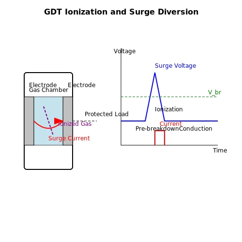
ຮູບທີ 2: ໂຄງສ້າງ ແລະ ພຶດຕິກໍາການເຮັດວຽກຂອງທໍ່ລະບາຍອາຍແກັສ (GDT). ແຜນວາດເບື້ອງຊ້າຍສະແດງໃຫ້ເຫັນໂຄງສ້າງພາຍໃນ: ຫ້ອງອາຍແກັສທີ່ຜະນຶກແໜ້ນດ້ວຍຊ່ອງຫວ່າງເອເລັກໂຕຣດ ແລະ ການບັນຈຸອາຍແກັສທີ່ບໍ່ມີປະຕິກິລິຍາ (argon/neon). ກຣາຟເບື້ອງຂວາສະແດງໃຫ້ເຫັນການຕອບສະໜອງການແຕກຕົວເປັນໄອອອນ—ເມື່ອແຮງດັນຊົ່ວຄາວເກີນຂອບເຂດໄຟຟ້າແຮງສູງ, ອາຍແກັສຈະແຕກຕົວເປັນໄອອອນສ້າງຊ່ອງທາງ plasma ທີ່ນໍາໄຟຟ້າໄດ້, ແຮງດັນຫຼຸດລົງເປັນໂໝດ arc (~10-20V), ແລະ ກະແສໄຟກະຊາກປ່ຽນທິດທາງຜ່ານ plasma ຈົນກວ່າກະແສໄຟຟ້າຈະຫຼຸດລົງຕໍ່າກວ່າຂອບເຂດການປ່ຽນແປງຈາກແສງເປັນ arc.
ໄດໂອດ TVS: ໂຄງສ້າງ ແລະ ຫຼັກການເຮັດວຽກ
ໄດໂອດ Transient Voltage Suppressor ແມ່ນອຸປະກອນ avalanche ຊິລິຄອນທີ່ຖືກອອກແບບສະເພາະສໍາລັບການຈໍາກັດໄຟກະຊາກ. ພວກເຂົາເຈົ້າສົມທົບເວລາຕອບສະໜອງທີ່ໄວທີ່ສຸດກັບແຮງດັນຈໍາກັດຕ່ໍາສຸດທີ່ມີຢູ່ໃນອົງປະກອບການປ້ອງກັນໄຟກະຊາກ, ເຮັດໃຫ້ພວກເຂົາເປັນທາງເລືອກທີ່ຕ້ອງການສໍາລັບການປົກປ້ອງວົງຈອນ semiconductor ທີ່ລະອຽດອ່ອນ.
内部结构
ໄດໂອດ TVS ໂດຍພື້ນຖານແລ້ວແມ່ນໄດໂອດ Zener ພິເສດທີ່ຖືກປັບປຸງໃຫ້ເໝາະສົມສໍາລັບພະລັງງານກໍາມະຈອນສູງແທນທີ່ຈະເປັນການຄວບຄຸມແຮງດັນ. ຊິລິຄອນມີຈຸດເຊື່ອມຕໍ່ P-N ທີ່ຖືກ doped ຢ່າງໜັກທີ່ຖືກອອກແບບມາເພື່ອເຂົ້າສູ່ການແຮງດັນໄຟຟ້າແຮງສູງ avalanche ຢູ່ແຮງດັນທີ່ຊັດເຈນ. ເນື້ອທີ່ຂອງຊິ້ນສ່ວນແມ່ນໃຫຍ່ກວ່າຕົວຄວບຄຸມ Zener ທີ່ທຽບເທົ່າຫຼາຍເພື່ອຮັບມືກັບກະແສສູງສຸດຂອງເຫດການໄຟກະຊາກ—ຫຼາຍຮ້ອຍແອມແປໃນກໍາມະຈອນ submicrosecond.
ຫຼັກການປະຕິບັດງານ
ພາຍໃຕ້ແຮງດັນໄຟຟ້າປະຕິບັດງານປົກກະຕິ, ໄດໂອດ TVS ເຮັດວຽກໃນການບ່ຽງເບນປີ້ນກັບກັນດ້ວຍການຮົ່ວໄຫຼໃນລະດັບນາໂນແອມແປເທົ່ານັ້ນ. ເມື່ອເຫດການຊົ່ວຄາວເກີນແຮງດັນໄຟຟ້າແຮງສູງປີ້ນກັບກັນ (V_BR), ຈຸດເຊື່ອມຕໍ່ຊິລິຄອນຈະເຂົ້າສູ່ການຄູນ avalanche. ການແຕກຕົວເປັນໄອອອນຂອງຜົນກະທົບສ້າງນໍ້າຖ້ວມຂອງຄູ່ເອເລັກໂຕຣນິກ-ຮູ, ແລະ ຄວາມຕ້ານທານຂອງຈຸດເຊື່ອມຕໍ່ຫຼຸດລົງ. ອຸປະກອນຈໍາກັດແຮງດັນຢູ່ລະດັບແຮງດັນໄຟຟ້າແຮງສູງບວກກັບຄວາມຕ້ານທານແບບໄດນາມິກຄູນກັບກະແສໄຟກະຊາກ.
ຟີຊິກແມ່ນຂອງແຂງຢ່າງດຽວໂດຍບໍ່ມີການເຄື່ອນໄຫວທາງກົນຈັກ, ການແຕກຕົວເປັນໄອອອນຂອງອາຍແກັສ, ຫຼື ການປ່ຽນແປງໄລຍະຂອງວັດສະດຸ. ນີ້ເຮັດໃຫ້ເວລາຕອບສະໜອງຢູ່ໃນລະດັບນາໂນວິນາທີ—ຕໍ່າກວ່າ 1 ns ສໍາລັບຊິລິຄອນເປົ່າ, ເຖິງແມ່ນວ່າ inductance ຂອງຊຸດໂດຍປົກກະຕິຈະຊຸກຍູ້ການຕອບສະໜອງທີ່ມີປະສິດທິພາບເປັນ 1-5 ns ສໍາລັບອຸປະກອນທີ່ໃຊ້ໄດ້. ຄຸນລັກສະນະແຮງດັນ-ກະແສແມ່ນຊັນຫຼາຍ (ຄວາມຕ້ານທານແບບໄດນາມິກຕໍ່າ), ໃຫ້ການຈໍາກັດທີ່ແໜ້ນໜາ.
关键参数与特性
ການຈັດອັນດັບພະລັງງານກໍາມະຈອນ: ຜູ້ຜະລິດ TVS ກໍານົດຄວາມສາມາດໃນການຮັບພະລັງງານໂດຍໃຊ້ຄວາມກວ້າງຂອງກໍາມະຈອນທີ່ໄດ້ມາດຕະຖານ (ໂດຍປົກກະຕິແມ່ນຮູບແບບຄື້ນ exponential 10/1000 µs). ຄອບຄົວຜະລິດຕະພັນທົ່ວໄປສະເໜີການຈັດອັນດັບກໍາມະຈອນ 400W, 600W, 1500W, ຫຼື 5000W. ຄວາມສາມາດໃນການຮັບກະແສສູງສຸດແມ່ນຄິດໄລ່ຈາກພະລັງງານກໍາມະຈອນ ແລະ ແຮງດັນຈໍາກັດ—ອຸປະກອນ 600W ທີ່ມີການຈໍາກັດ 15V ສາມາດຮັບມືກັບກະແສສູງສຸດປະມານ 40A.
ປະສິດທິພາບການຈໍາກັດ: ໄດໂອດ TVS ສະເໜີແຮງດັນຈໍາກັດຕ່ໍາສຸດຂອງເຕັກໂນໂລຢີການປ້ອງກັນໄຟກະຊາກໃດໆ. ອັດຕາສ່ວນຂອງແຮງດັນຈໍາກັດຕໍ່ແຮງດັນຢຸດ (V_C/V_WM) ໂດຍປົກກະຕິແມ່ນ 1.3 ຫາ 1.5, ເມື່ອທຽບກັບ 2.0-2.5 ສໍາລັບ MOVs. ການຄວບຄຸມທີ່ແໜ້ນໜານີ້ແມ່ນມີຄວາມສໍາຄັນສໍາລັບການປົກປ້ອງໂລຈິກ 3.3V, USB 5V, ວົງຈອນລົດຍົນ 12V, ແລະ ໂຫຼດອື່ນໆທີ່ລະອຽດອ່ອນຕໍ່ແຮງດັນ.
ຄວາມຈຸ: ຄວາມຈຸ TVS ແຕກຕ່າງກັນຢ່າງກວ້າງຂວາງກັບການກໍ່ສ້າງອຸປະກອນ. ໄດໂອດ TVS ຈຸດເຊື່ອມຕໍ່ມາດຕະຖານສາມາດສະແດງໃຫ້ເຫັນຫຼາຍຮ້ອຍ picofarads, ເຊິ່ງໂຫຼດສາຍຂໍ້ມູນຄວາມໄວສູງ. ຄອບຄົວ TVS ຄວາມຈຸຕ່ໍາທີ່ຖືກອອກແບບມາສໍາລັບ HDMI, USB 3.0, Ethernet, ແລະ RF ໃຊ້ເລຂາຄະນິດຂອງຈຸດເຊື່ອມຕໍ່ພິເສດ ແລະ ບັນລຸຕໍ່າກວ່າ 5 pF ຕໍ່ສາຍ.
ການເຖົ້າແກ່ ແລະ ຄວາມໜ້າເຊື່ອຖື: ບໍ່ເຫມືອນກັບ MOVs, ໄດໂອດ TVS ສະແດງໃຫ້ເຫັນເຖິງການປ່ຽນແປງປະສິດທິພາບໜ້ອຍທີ່ສຸດພາຍໃຕ້ຄວາມກົດດັນກໍາມະຈອນທີ່ຖືກຈັດອັນດັບ. ຈຸດເຊື່ອມຕໍ່ຊິລິຄອນບໍ່ໄດ້ເສື່ອມໂຊມສະສົມຈາກໄຟກະຊາກຊໍ້າໆພາຍໃນການຈັດອັນດັບ. ຮູບແບບຄວາມລົ້ມເຫຼວໂດຍປົກກະຕິແມ່ນວົງຈອນເປີດ (ການທໍາລາຍຈຸດເຊື່ອມຕໍ່) ຫຼື ວົງຈອນສັ້ນ (ການເຊື່ອມໂລຫະ), ທັງສອງຢ່າງເກີດຂຶ້ນພາຍໃຕ້ການໂຫຼດເກີນທີ່ຮ້າຍແຮງທີ່ເກີນການຈັດອັນດັບ.
ຄໍາຮ້ອງສະຫມັກທົ່ວໄປ: ການປ້ອງກັນວົງຈອນລະດັບກະດານ (ພອດ I/O, ທາງລົດໄຟພະລັງງານ), ອິນເຕີເຟດ USB ແລະ HDMI, ເອເລັກໂຕຣນິກລົດຍົນ, ການສະໜອງພະລັງງານ DC, ສາຍຂໍ້ມູນການສື່ສານ, ແລະ ການນໍາໃຊ້ໃດໆທີ່ຕ້ອງການການຕອບສະໜອງທີ່ໄວ ແລະ ການຈໍາກັດແຮງດັນທີ່ແໜ້ນໜາສໍາລັບໂຫຼດ semiconductor.
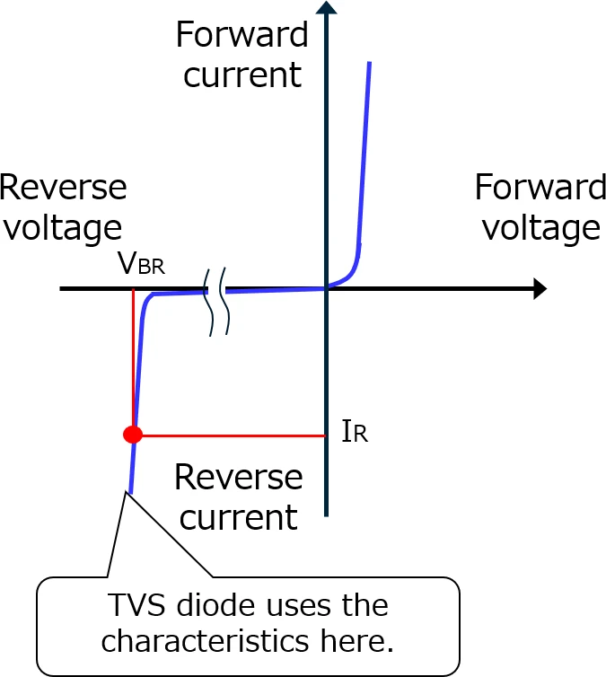
ຮູບທີ 3: ເສັ້ນໂຄ້ງຄຸນລັກສະນະແຮງດັນ-ກະແສ (I-V) ຂອງໄດໂອດ TVS ສະແດງໃຫ້ເຫັນການເຮັດວຽກຂອງ semiconductor avalanche. ພາຍໃຕ້ແຮງດັນປົກກະຕິ (ພາກພື້ນຢຸດ V_WM), ອຸປະກອນຮັກສາຄວາມຕ້ານທານສູງດ້ວຍການຮົ່ວໄຫຼນາໂນແອມແປ. ເມື່ອເຫດການຊົ່ວຄາວເກີນແຮງດັນໄຟຟ້າແຮງສູງປີ້ນກັບກັນ (V_BR), ຈຸດເຊື່ອມຕໍ່ P-N ຊິລິຄອນຈະເຂົ້າສູ່ການຄູນ avalanche—ຄວາມຕ້ານທານຂອງຈຸດເຊື່ອມຕໍ່ຫຼຸດລົງ ແລະ ອຸປະກອນຈໍາກັດແຮງດັນຢູ່ V_C (ແຮງດັນໄຟຟ້າແຮງສູງບວກກັບຄວາມຕ້ານທານແບບໄດນາມິກ × ກະແສໄຟກະຊາກ). ເສັ້ນໂຄ້ງທີ່ຊັນ (ຄວາມຕ້ານທານແບບໄດນາມິກຕໍ່າ) ໃຫ້ການຄວບຄຸມແຮງດັນທີ່ແໜ້ນໜາເຊິ່ງມີຄວາມສໍາຄັນສໍາລັບການປົກປ້ອງໂຫຼດ semiconductor.
ການຈໍາກັດທຽບກັບ Crowbar: ສອງປັດຊະຍາການປ້ອງກັນ
ຄວາມແຕກຕ່າງພື້ນຖານລະຫວ່າງເຕັກໂນໂລຢີເຫຼົ່ານີ້ແມ່ນຢູ່ໃນປັດຊະຍາການປ້ອງກັນຂອງພວກເຂົາ. MOVs ແລະ ໄດໂອດ TVS ແມ່ນ ອຸປະກອນຈໍາກັດ—ພວກເຂົາຈໍາກັດແຮງດັນໃຫ້ຢູ່ໃນລະດັບສະເພາະທີ່ເປັນອັດຕາສ່ວນກັບກະແສໄຟກະຊາກ. GDTs ແມ່ນ ອຸປະກອນ crowbar—ພວກເຂົາສ້າງວົງຈອນສັ້ນທີ່ຫຼຸດແຮງດັນລົງເປັນລະດັບທີ່ເຫຼືອຕ່ໍາໂດຍບໍ່ຄໍານຶງເຖິງຂະໜາດຂອງກະແສ.
ພຶດຕິກໍາການຈໍາກັດ (MOV ແລະ TVS): ເມື່ອກະແສໄຟກະຊາກເພີ່ມຂຶ້ນ, ແຮງດັນຈໍາກັດເພີ່ມຂຶ້ນຕາມເສັ້ນໂຄ້ງ V-I ທີ່ບໍ່ເປັນເສັ້ນຊື່ຂອງອຸປະກອນ. MOV ທີ່ຖືກຈັດອັນດັບ 275V RMS ອາດຈະຈໍາກັດຢູ່ 750V ສໍາລັບໄຟກະຊາກ 1 kA ແຕ່ເພີ່ມຂຶ້ນເປັນ 900V ທີ່ 5 kA. ໄດໂອດ TVS ທີ່ຖືກຈັດອັນດັບ 15V standoff ອາດຈະຈໍາກັດຢູ່ 24V ສໍາລັບ 10A ແຕ່ບັນລຸ 26V ທີ່ 20A. ໂຫຼດທີ່ຖືກປົກປ້ອງເຫັນແຮງດັນທີ່ກໍານົດໂດຍຂະໜາດຂອງໄຟກະຊາກ ແລະ ຄຸນລັກສະນະຂອງອຸປະກອນ.
ພຶດຕິກໍາ Crowbar (GDT): ເມື່ອການແຮງດັນໄຟຟ້າແຮງສູງເກີດຂຶ້ນ, GDT ຈະເຂົ້າສູ່ໂໝດ arc ແລະ ແຮງດັນຫຼຸດລົງເປັນ 10-20V ໂດຍບໍ່ຄໍານຶງເຖິງວ່າກະແສໄຟກະຊາກແມ່ນ 100A ຫຼື 10,000A. ນີ້ໃຫ້ການປົກປ້ອງທີ່ດີເລີດເມື່ອຖືກກະຕຸ້ນ, ແຕ່ການໄຟຟ້າແຮງສູງເບື້ອງຕົ້ນສາມາດອະນຸຍາດໃຫ້ມີແຮງດັນໄຟຟ້າກ່ອນທີ່ການແຕກຕົວເປັນໄອອອນຈະສໍາເລັດ. ນີ້ແມ່ນເຫດຜົນທີ່ວ່າໂຫຼດທີ່ລະອຽດອ່ອນທີ່ຢູ່ເບື້ອງຫຼັງ GDTs ມັກຈະຕ້ອງການຕົວຈໍາກັດທີ່ໄວກວ່າອັນທີສອງ.
ແຕ່ລະປັດຊະຍາເໝາະສົມກັບການນໍາໃຊ້ທີ່ແຕກຕ່າງກັນ. ອຸປະກອນຈໍາກັດປົກປ້ອງໂດຍການຈໍາກັດການສໍາຜັດກັບແຮງດັນ. ອຸປະກອນ Crowbar ປົກປ້ອງໂດຍການປ່ຽນທິດທາງກະແສ. ການຈໍາກັດເຮັດວຽກເມື່ອວົງຈອນທີ່ຖືກປົກປ້ອງສາມາດທົນທານຕໍ່ແຮງດັນຈໍາກັດ. Crowbar ເຮັດວຽກເມື່ອແຫຼ່ງໄຟກະຊາກມີຄວາມຕ້ານທານສູງພໍທີ່ການເຮັດໃຫ້ສາຍສັ້ນບໍ່ທໍາລາຍອຸປະກອນຂັ້ນເທິງ ຫຼື ເຮັດໃຫ້ເກີດບັນຫາກະແສຕິດຕາມ.
MOV ທຽບກັບ GDT ທຽບກັບ TVS: ການປຽບທຽບຂ້າງຄຽງ
ຕາຕະລາງຂ້າງລຸ່ມນີ້ກໍານົດຄວາມແຕກຕ່າງຂອງປະສິດທິພາບທີ່ສໍາຄັນໃນທົ່ວສາມເຕັກໂນໂລຢີການປ້ອງກັນໄຟກະຊາກເຫຼົ່ານີ້:
| ພາລາມິເຕີ | MOV (Metal Oxide Varistor) | GDT (ທໍ່ລະບາຍອາຍແກັສ) | TVS Diode |
| ຫຼັກການປະຕິບັດງານ | ຄວາມຕ້ານທານທີ່ບໍ່ເປັນເສັ້ນຊື່ທີ່ຂຶ້ນກັບແຮງດັນ (ຂອບເຂດເມັດ ZnO) | Crowbar ການແຕກຕົວເປັນໄອອອນຂອງອາຍແກັສ | ການແຮງດັນໄຟຟ້າແຮງສູງ avalanche ຂອງ semiconductor |
| ກົນໄກການປົກປ້ອງ | ການຈໍາກັດ | Crowbar | ການຈໍາກັດ |
| ເວລາຕອບສະຫນອງ | <25 ns (ສ່ວນລາຍການປົກກະຕິ) | 100 ns – 1 µs (ຂຶ້ນກັບແຮງດັນ) | 1-5 ns (ຈໍາກັດໂດຍຊຸດ) |
| ແຮງດັນຈໍາກັດ/Arc | 2.0-2.5 × MCOV | 10-20 V (ໂໝດ arc) | 1.3-1.5 × V_standoff |
| ກະແສໄຟກະຊາກ (8/20 µs) | 400 A – 100 kA (ຂຶ້ນກັບຂະໜາດ) | 5 kA – 20 kA (ລະດັບໂທລະຄົມ) | 10 A – 200 A (ຄອບຄົວ 600W ~40A) |
| 能量耐受 | ດີເລີດ (100-1000 J) | ດີເລີດ (ພລາສມາແຈກຢາຍ) | ປານກາງ (ຈຳກັດໂດຍຈຸດເຊື່ອມຕໍ່) |
| ຄວາມຈຸ | 50-5000 pF (ຂຶ້ນກັບພື້ນທີ່) | <2 pF | 5-500 pF (ຂຶ້ນກັບໂຄງສ້າງ) |
| ພຶດຕິກຳການເສື່ອມສະພາບ | ເສື່ອມລົງຕາມຮອບວຽນແຮງດັນເກີນ; V_n ເລື່ອນລົງ | ຄົງທີ່ຕະຫຼອດແຮງດັນເກີນຫຼາຍພັນຄັ້ງ | ການເລື່ອນໜ້ອຍທີ່ສຸດພາຍໃນຂອບເຂດທີ່ກຳນົດ |
| ຮູບແບບຄວາມລົ້ມເຫຼວ | ການເສື່ອມສະພາບ → ລັດວົງຈອນສັ້ນ ຫຼື ເປີດ | ລັດວົງຈອນສັ້ນ (ຮັກສາການເກີດປະກາຍໄຟ) | ເປີດ ຫຼື ລັດວົງຈອນສັ້ນ (ຮ້າຍແຮງເທົ່ານັ້ນ) |
| ຄວາມສ່ຽງຕໍ່ກະແສໄຟຟ້າຕິດຕາມ | ຕ່ຳ (ດັບເອງ) | ສູງ (ຕ້ອງການການຈຳກັດພາຍນອກ) | ບໍ່ມີ (ສະຖານະແຂງ) |
| ຊ່ວງແຮງດັນໄຟຟ້າປົກກະຕິ | 18V RMS – 1000V RMS | 75V – 5000V DC sparkover | 3.3V – 600V standoff |
| ຄ່າໃຊ້ຈ່າຍ (ທຽບເທົ່າ) | ຕ່ຳ ($0.10 – $5) | ຕ່ຳ-ປານກາງ ($0.50 – $10) | ຕ່ຳ-ປານກາງ ($0.20 – $8) |
| ມາດຕະຖານ | IEC 61643-11, UL 1449 | ITU-T K.12, IEEE C62.31 | IEC 61643-11, UL 1449 |
| ຖອງ | ສາຍໄຟ AC, ການແຈກຢາຍພະລັງງານ, ອຸດສາຫະກໍາ | ສາຍໂທລະຄົມ, ຂໍ້ມູນຄວາມໄວສູງ, ເສົາອາກາດ | I/O ລະດັບແຜງວົງຈອນ, ແຫຼ່ງຈ່າຍໄຟ DC, ຍານຍົນ |
ຂໍ້ຄິດທີ່ສໍາຄັນຈາກການປຽບທຽບ
MOVs ໃຫ້ຄວາມສົມດຸນທີ່ດີທີ່ສຸດຂອງການຈັດການພະລັງງານ, ການຕອບສະໜອງໄວ, ແລະ ຄ່າໃຊ້ຈ່າຍສໍາລັບແຮງດັນເກີນລະດັບພະລັງງານ. ພວກມັນເດັ່ນໃນການປ້ອງກັນສາຍໄຟ AC ແຕ່ປະສົບບັນຫາຈາກການໂຫຼດຄາປາຊິເຕີໃນວົງຈອນຄວາມຖີ່ສູງ ແລະ ການເສື່ອມສະພາບສະສົມພາຍໃຕ້ຄວາມກົດດັນຊ້ຳໆ.
GDTs ເດັ່ນບ່ອນທີ່ການໂຫຼດສາຍໜ້ອຍທີ່ສຸດເປັນສິ່ງສໍາຄັນ ແລະ ຄວາມສາມາດໃນການຮັບກະແສໄຟຟ້າເກີນຕ້ອງໄດ້ຮັບການເພີ່ມປະສິດທິພາບສູງສຸດ. ຄາປາຊິເຕີຕໍ່າສຸດຂອງພວກມັນເຮັດໃຫ້ພວກມັນບໍ່ສາມາດປ່ຽນແທນໄດ້ໃນແອັບພລິເຄຊັນໂທລະຄົມ ແລະ RF, ແຕ່ການຕອບສະໜອງຊ້າກວ່າ ແລະ ຄວາມສ່ຽງຕໍ່ກະແສໄຟຟ້າຕິດຕາມຮຽກຮ້ອງໃຫ້ມີການອອກແບບວົງຈອນຢ່າງລະມັດລະວັງ.
TVS diodes ໃຫ້ການຈັບຍຶດທີ່ໄວທີ່ສຸດ ແລະ ແໜ້ນໜາທີ່ສຸດສໍາລັບອຸປະກອນເອເລັກໂຕຣນິກທີ່ລະອຽດອ່ອນ. ພວກມັນເປັນທາງເລືອກທີ່ໃຊ້ໄດ້ພຽງຢ່າງດຽວສໍາລັບການປົກປ້ອງ I/O ເຄິ່ງຕົວນໍາໃນແຮງດັນໄຟຟ້າຕ່ຳກວ່າ 50V, ແຕ່ຄວາມສາມາດດ້ານພະລັງງານຈຳກັດໝາຍຄວາມວ່າພວກມັນບໍ່ສາມາດຈັດການກັບແຮງດັນເກີນລະດັບຟ້າຜ່າທີ່ MOVs ແລະ GDTs ດູດຊຶມໄດ້ເປັນປະຈຳ.
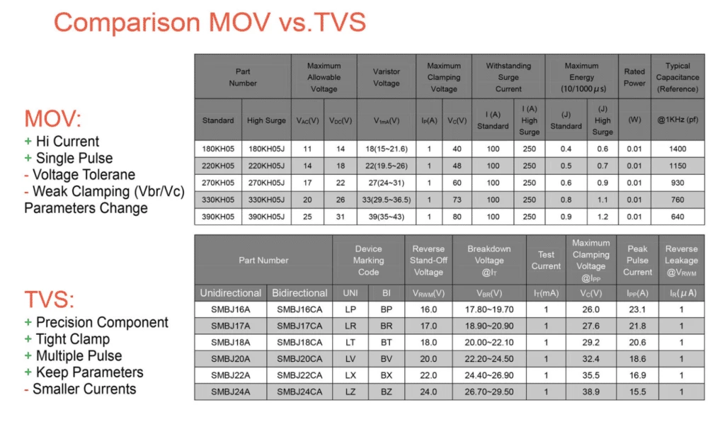
ຮູບທີ 4: ຕາຕະລາງປຽບທຽບແບບມືອາຊີບທີ່ກົງກັນຂ້າມກັບເຕັກໂນໂລຢີ MOV (Metal Oxide Varistor) ແລະ TVS (Transient Voltage Suppressor) ໃນທົ່ວສະເພາະທີ່ສໍາຄັນ. MOVs ສະແດງອັດຕາສ່ວນແຮງດັນໄຟຟ້າຈັບຍຶດທີ່ສູງກວ່າ (2.0-2.5× MCOV) ດ້ວຍການດູດຊຶມພະລັງງານທີ່ດີເລີດສໍາລັບແຮງດັນເກີນລະດັບພະລັງງານ, ໃນຂະນະທີ່ TVS diodes ໃຫ້ການຄວບຄຸມແຮງດັນໄຟຟ້າທີ່ແໜ້ນໜາກວ່າ (1.3-1.5× standoff) ດ້ວຍການຕອບສະໜອງທີ່ໄວກວ່າ (<5 ns) ສໍາລັບການປົກປ້ອງເຄິ່ງຕົວນໍາ. ຕາຕະລາງປະກອບມີລະດັບແຮງດັນໄຟຟ້າ, ຄວາມສາມາດໃນການຮັບກະແສໄຟຟ້າເກີນ, ແລະ ຕົວຢ່າງໝາຍເລກສ່ວນປົກກະຕິທີ່ສະແດງໃຫ້ເຫັນເຖິງຊອງປະສິດທິພາບທີ່ສົມບູນຂອງແຕ່ລະເຕັກໂນໂລຢີ.
ຄູ່ມືການເລືອກເຕັກໂນໂລຢີ: ເວລາທີ່ຈະໃຊ້ແຕ່ລະອັນ
ການເລືອກເຕັກໂນໂລຢີປ້ອງກັນແຮງດັນເກີນທີ່ຖືກຕ້ອງແມ່ນຂຶ້ນກັບການຈັບຄູ່ຄຸນລັກສະນະຂອງອຸປະກອນກັບຄວາມຕ້ອງການຂອງວົງຈອນ. ນີ້ແມ່ນກອບການຕັດສິນໃຈ:
ໃຊ້ MOV ເມື່ອ:
- ແຮງດັນໄຟຟ້າຂອງວົງຈອນແມ່ນສາຍໄຟ AC ຫຼື DC ແຮງດັນໄຟຟ້າສູງ (>50V): MOVs ມີຢູ່ໃນລະດັບແຮງດັນໄຟຟ້າຈາກ 18V RMS ຫາຫຼາຍກວ່າ 1000V, ເໝາະສົມຢ່າງສົມບູນກັບທີ່ຢູ່ອາໄສ (120/240V), ການຄ້າ (277/480V), ແລະ ການແຈກຢາຍພະລັງງານອຸດສາຫະກໍາ.
- ພະລັງງານແຮງດັນເກີນແມ່ນສູງ: ແຮງດັນເກີນທີ່ເກີດຈາກຟ້າຜ່າ, ການປ່ຽນແປງຊົ່ວຄາວຂອງການປ່ຽນສາຍໄຟ, ແລະ ກະແສໄຟຟ້າເຂົ້າຂອງມໍເຕີສ້າງລະດັບພະລັງງານ (ຫຼາຍຮ້ອຍຫາຫຼາຍພັນຈູນ) ທີ່ພຽງແຕ່ MOVs ສາມາດດູດຊຶມໄດ້ຢ່າງປະຫຍັດ.
- ເວລາຕອບສະໜອງ <25 ns ເປັນທີ່ຍອມຮັບໄດ້: ອຸປະກອນເອເລັກໂຕຣນິກພະລັງງານ ແລະ ອຸປະກອນອຸດສາຫະກໍາສ່ວນໃຫຍ່ທົນທານຕໍ່ຄວາມໄວໃນການຕອບສະໜອງຂອງ MOV.
- ການໂຫຼດຄາປາຊິເຕີເປັນທີ່ຍອມຮັບໄດ້: ຢູ່ທີ່ຄວາມຖີ່ຂອງພະລັງງານ (50/60 Hz), ເຖິງແມ່ນວ່າຄາປາຊິເຕີ 1000 pF ກໍ່ບໍ່ມີຜົນກະທົບ.
- ຄ່າໃຊ້ຈ່າຍຖືກຈຳກັດ: MOVs ສະເໜີຄ່າໃຊ້ຈ່າຍຕ່ຳສຸດຕໍ່ຈູນຂອງການປ້ອງກັນ.
ຫຼີກເວັ້ນ MOVs ເມື່ອ ປົກປ້ອງສາຍສື່ສານຄວາມໄວສູງ (ການໂຫຼດຄາປາຊິເຕີ), ວົງຈອນເຄິ່ງຕົວນໍາແຮງດັນໄຟຟ້າຕ່ຳ (ແຮງດັນໄຟຟ້າຈັບຍຶດສູງເກີນໄປ), ຫຼື ແອັບພລິເຄຊັນທີ່ຕ້ອງການປະສິດທິພາບທີ່ບໍ່ມີການເລື່ອນຮັບປະກັນຕະຫຼອດຫຼາຍທົດສະວັດ (ຄວາມກັງວົນກ່ຽວກັບການເສື່ອມສະພາບ).
ໃຊ້ GDT ເມື່ອ:
- ການໂຫຼດສາຍຕ້ອງໜ້ອຍທີ່ສຸດ (<2 pF): ໂມເດັມ xDSL, ສາຍເຄເບິນບຣອດແບນ, Gigabit Ethernet, ເຄື່ອງຮັບ RF, ແລະ ອິນພຸດເສົາອາກາດບໍ່ສາມາດທົນທານຕໍ່ຄາປາຊິເຕີຂອງ MOVs ຫຼື ອຸປະກອນ TVS ມາດຕະຖານໄດ້.
- ຄວາມສາມາດໃນການຮັບກະແສໄຟຟ້າເກີນຕ້ອງໄດ້ຮັບການເພີ່ມປະສິດທິພາບສູງສຸດ: ສໍານັກງານໃຫຍ່ໂທລະຄົມ, ເສົາສັນຍານໂທລະສັບມືຖື, ແລະ ການຕິດຕັ້ງກາງແຈ້ງປະເຊີນກັບແຮງດັນເກີນຟ້າຜ່າທີ່ມີແอมພລິຈູດສູງຊ້ຳໆທີ່ເກີນລະດັບ TVS.
- ວົງຈອນທີ່ໄດ້ຮັບການປົກປ້ອງມີອິມພີແດນສ໌ແຫຼ່ງສູງ: ສາຍໂທລະສັບ (600Ω), ສາຍປ້ອນເສົາອາກາດ (50-75Ω), ແລະ ສາຍເຄເບິນຂໍ້ມູນສາມາດຖືກລັດວົງຈອນສັ້ນໄດ້ຢ່າງປອດໄພໂດຍບໍ່ມີກະແສໄຟຟ້າຕິດຕາມຫຼາຍເກີນໄປ.
- ແຮງດັນໄຟຟ້າປະຕິບັດງານແມ່ນສູງ (>100V): GDTs ມີໃຫ້ກັບແຮງດັນໄຟຟ້າ sparkover ຈາກ 75V ຫາ 5000V, ກວມເອົາແຮງດັນໄຟຟ້າໂທລະຄົມ, PoE (Power over Ethernet), ແລະ ການສົ່ງສັນຍານແຮງດັນໄຟຟ້າສູງ.
ຫຼີກເວັ້ນ GDTs ເມື່ອ ປົກປ້ອງແຫຼ່ງຈ່າຍໄຟ DC ອິມພີແດນສ໌ຕ່ຳ (ຄວາມສ່ຽງຕໍ່ກະແສໄຟຟ້າຕິດຕາມ), ວົງຈອນທີ່ຕ້ອງການການຕອບສະໜອງທີ່ໄວທີ່ສຸດ (<100 ns ທີ່ສໍາຄັນ), ຫຼື ໂຫຼດທີ່ອ່ອນໄຫວຕໍ່ແຮງດັນໄຟຟ້າທີ່ບໍ່ສາມາດທົນທານຕໍ່ການກະຕຸ້ນ spark-over ເບື້ອງຕົ້ນ (ຕ້ອງການການຈັບຍຶດຂັ້ນສອງ).
ໃຊ້ TVS Diode ເມື່ອ:
- ແຮງດັນໄຟຟ້າທີ່ຈັບຕ້ອງໄດ້ຕ້ອງຖືກຄວບຄຸມຢ່າງເຂັ້ມງວດ: ລະບົບໂລຈິກ 3.3V, USB 5V, ວົງຈອນລົດຍົນ 12V, ແລະການໂຫຼດ semiconductor ອື່ນໆຕ້ອງການການຈັບພາຍໃນ 20-30% ຂອງແຮງດັນໄຟຟ້າທີ່ກໍານົດ—ມີພຽງແຕ່ diodes TVS ເທົ່ານັ້ນທີ່ໃຫ້ສິ່ງນີ້.
- ເວລາຕອບສະໜອງຕ້ອງໄວທີ່ສຸດ (<5 ns): ການປົກປ້ອງໂປເຊດເຊີຄວາມໄວສູງ, FPGAs, ແລະວົງຈອນອະນາລັອກທີ່ລະອຽດອ່ອນຕ້ອງການການຕອບສະໜອງໃນລະດັບນາໂນວິນາທີ.
- ແຮງດັນໄຟຟ້າຂອງວົງຈອນແມ່ນຕໍ່າຫາປານກາງ (<100V): ຄອບຄົວ TVS ກວມເອົາທຸກສິ່ງທຸກຢ່າງຈາກສາຍຂໍ້ມູນ 3.3V ໄປຫາເຄື່ອງສະໜອງໂທລະຄົມ 48V.
- ບໍ່ສາມາດທົນທານຕໍ່ການແກ່/ເລື່ອນໄດ້: ອຸປະກອນການແພດ, ການບິນອະວະກາດ, ແລະລະບົບທີ່ສໍາຄັນຕໍ່ຄວາມປອດໄພຕ້ອງການການປົກປ້ອງທີ່ຄາດເດົາໄດ້, ໝັ້ນຄົງຕະຫຼອດອາຍຸການໃຊ້ງານຂອງຜະລິດຕະພັນ.
- ພື້ນທີ່ກະດານມີຈໍາກັດ: ອຸປະກອນ SMT TVS ໃນຊຸດ 0402 ຫຼື SOT-23 ເໝາະສົມກັບບ່ອນທີ່ MOVs ແລະ GDTs ບໍ່ສາມາດເຮັດໄດ້.
ຫຼີກເວັ້ນ diodes TVS ເມື່ອ ພະລັງງານກະແສເກີນອັດຕາພະລັງງານກໍາມະຈອນ (ອຸປະກອນ 600W ປົກກະຕິດູດຊຶມພຽງແຕ່ ~1 joule), ກະແສໄຟຟ້າເກີນອັດຕາສູງສຸດ (40A ປົກກະຕິສໍາລັບ 600W ທີ່ 15V), ຫຼືຄ່າໃຊ້ຈ່າຍຕໍ່ຊ່ອງທາງກາຍເປັນສິ່ງຫ້າມໃນລະບົບຫຼາຍສາຍ.
ມາຕຣິກເບື້ອງການຕັດສິນໃຈ
| ຄໍາຮ້ອງສະຫມັກ | ເຕັກໂນໂລຢີຫຼັກ | ເຫດຜົນ |
| ການປ້ອງກັນແຜງໄຟ AC | MOV (Type 1/2 SPD) | ພະລັງງານສູງ, 120-480V, ປະຫຍັດຄ່າໃຊ້ຈ່າຍ |
| ສ່ວນຕິດຕໍ່ສາຍໂທລະຄົມ | GDT + TVS (ຂັ້ນຕອນ) | GDT ດູດຊຶມພະລັງງານ, TVS ຈັບສິ່ງທີ່ເຫຼືອ |
| ສາຍຂໍ້ມູນ USB 2.0 / 3.0 | TVS ຄວາມຈຸຕ່ຳ | ຂອບໄວ, ການສະໜອງ 5V, ຕ້ອງການ <5 pF |
| Ethernet (10/100/1000 Base-T) | GDT (ຂັ້ນຕົ້ນ) + TVS ຄວາມຈຸຕ່ຳ | ການໂຫຼດໜ້ອຍທີ່ສຸດ, ການສໍາຜັດກັບກະແສໄຟຟ້າສູງ |
| 24V DC ອຸດສາຫະກໍາ I/O | TVS | ການຈັບທີ່ແໜ້ນໜາ, ການຕອບສະໜອງໄວ, ບໍ່ມີການແກ່ |
| PV ແສງຕາເວັນ DC input | MOV (DC-rated) | ແຮງດັນໄຟຟ້າສູງ (600-1000V), ພະລັງງານສູງ |
| ວົງຈອນລົດຍົນ 12V | TVS | ການປ້ອງກັນການຖິ້ມການໂຫຼດ, ການຈັບທີ່ແໜ້ນໜາທີ່ 24-36V |
| RF antenna input | GDT | Sub-2 pF, ການຈັດການພະລັງງານສູງ |
| 3.3V FPGA power rail | TVS (ຄວາມຈຸຕ່ຳ) | ການຈັບ 6-8V, ການຕອບສະໜອງ <1 ns ທີ່ສໍາຄັນ |
ຕາຕະລາງນີ້ແມ່ນຈຸດເລີ່ມຕົ້ນ. ການຕິດຕັ້ງທີ່ສັບສົນມັກຈະລວມເອົາເຕັກໂນໂລຢີໃນໂຄງການປ້ອງກັນຊັ້ນ, ໃຊ້ປະໂຫຍດຈາກຄວາມເຂັ້ມແຂງຂອງແຕ່ລະຂັ້ນຕອນ.
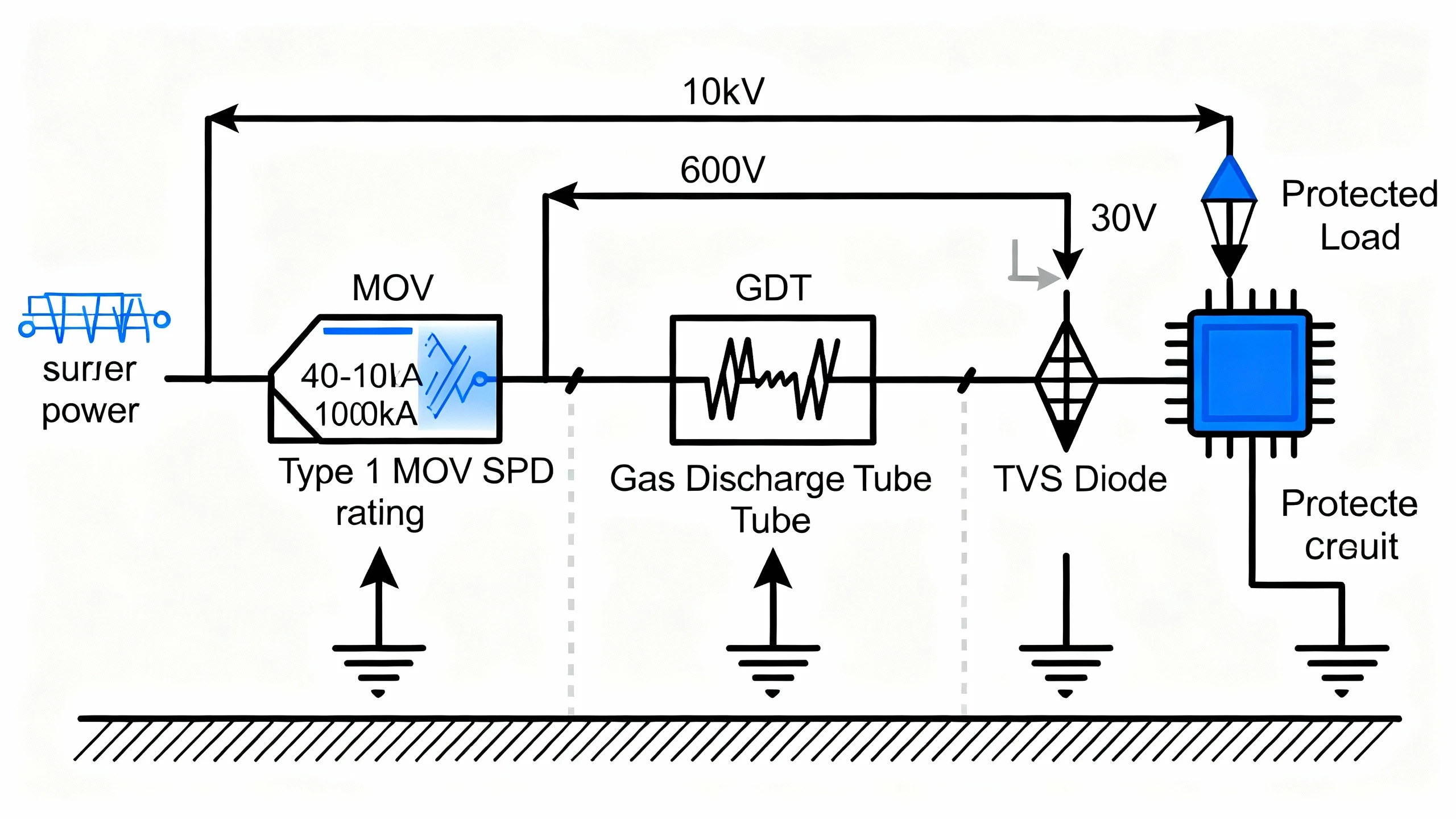
ຮູບທີ 5: ແຜນວາດສະຖາປັດຕະຍະກໍາການປ້ອງກັນກະແສໄຟຟ້າສາມຂັ້ນຕອນແບບມືອາຊີບທີ່ສະແດງໃຫ້ເຫັນເຖິງຍຸດທະສາດການປ້ອງກັນທີ່ປະສານງານກັນ. ຂັ້ນຕອນທີ 1 (ຂັ້ນຕົ້ນ): Type 1 MOV SPD ຢູ່ທາງເຂົ້າບໍລິການຈັດການພະລັງງານກະແສໄຟຟ້າທີ່ຮຸນແຮງ (40-100 kA) ແລະຈັບແຮງດັນຈາກ 10+ kV ຫາ ~600V. ຂັ້ນຕອນທີ 2 (ຂັ້ນສອງ): Gas Discharge Tube ປ່ຽນເສັ້ນທາງ transients ແຮງດັນໄຟຟ້າສູງທີ່ເຫຼືອແລະຫຼຸດຜ່ອນແຮງດັນໄຟຟ້າເປັນ ~30V ຜ່ານການດໍາເນີນງານຮູບແບບ arc. ຂັ້ນຕອນທີ 3 (ສຸດທ້າຍ): TVS diode ໃຫ້ການຈັບທີ່ແໜ້ນໜາ (<1.5× ແຮງດັນໄຟຟ້າ standoff) ດ້ວຍການຕອບສະໜອງໃນລະດັບນາໂນວິນາທີເພື່ອປົກປ້ອງການໂຫຼດ semiconductor ທີ່ລະອຽດອ່ອນ. ແຕ່ລະຂັ້ນຕອນມີການຕໍ່ສາຍດິນທີ່ເໝາະສົມ ແລະການປະສານງານແຮງດັນໄຟຟ້າເພື່ອຮັບປະກັນວ່າອຸປະກອນຕົ້ນນໍ້າກະຕຸ້ນກ່ອນອົງປະກອບປາຍນໍ້າ, ສ້າງຈຸດ “handoff” ທີ່ຊັດເຈນທີ່ແຈກຢາຍພະລັງງານກະແສໄຟຟ້າໃນທົ່ວ cascade ການປ້ອງກັນ. ວິທີການເປັນຊັ້ນນີ້ໃຊ້ປະໂຫຍດຈາກຄວາມເຂັ້ມແຂງທີ່ສົມບູນຂອງເຕັກໂນໂລຢີ MOV (ພະລັງງານສູງ), GDT (ຄວາມຈຸຕ່ຳ), ແລະ TVS (ການຈັບທີ່ແໜ້ນໜາ).
ການປ້ອງກັນເປັນຊັ້ນ: ການລວມເຕັກໂນໂລຢີ
ສະຖາປັດຕະຍະກໍາການປ້ອງກັນກະແສໄຟຟ້າທີ່ເຂັ້ມແຂງທີ່ສຸດບໍ່ໄດ້ອີງໃສ່ເຕັກໂນໂລຢີດຽວ. ແທນທີ່ຈະ, ພວກເຂົາປະສານງານຫຼາຍຂັ້ນຕອນ, ແຕ່ລະຂັ້ນຕອນຖືກປັບໃຫ້ເໝາະສົມກັບສ່ວນທີ່ແຕກຕ່າງກັນຂອງ spectrum ໄພຂົ່ມຂູ່. ວິທີການ “ປ້ອງກັນໃນຄວາມເລິກ” ນີ້ໃຊ້ປະໂຫຍດຈາກຄວາມເຂັ້ມແຂງທີ່ສົມບູນຂອງເຕັກໂນໂລຢີ MOV, GDT, ແລະ TVS.
ເປັນຫຍັງຕ້ອງປ້ອງກັນເປັນຊັ້ນ?
ການແຈກຢາຍພະລັງງານ: TVS diode ດຽວບໍ່ສາມາດດູດຊຶມກະແສໄຟຟ້າ 10 kA ໄດ້, ແຕ່ GDT ຕົ້ນນໍ້າສາມາດປ່ຽນເສັ້ນທາງ 99% ຂອງພະລັງງານນັ້ນ, ເຮັດໃຫ້ TVS ຈັບສິ່ງທີ່ເຫຼືອ. ແຕ່ລະຂັ້ນຕອນຈັດການສິ່ງທີ່ມັນເຮັດໄດ້ດີທີ່ສຸດ.
ການເພີ່ມປະສິດທິພາບຄວາມໄວ: GDT ໃຊ້ເວລາຫຼາຍຮ້ອຍນາໂນວິນາທີເພື່ອແຕກຕົວເປັນໄອອອນ. ໃນລະຫວ່າງເວລານັ້ນ, TVS ໄວປາຍນໍ້າສາມາດຈັບ spike ເບື້ອງຕົ້ນ, ປ້ອງກັນຄວາມເສຍຫາຍຕໍ່ການໂຫຼດທີ່ລະອຽດອ່ອນ. ເມື່ອ GDT ເຮັດວຽກ, ມັນຈະຮັບໜ້າທີ່ປ່ຽນເສັ້ນທາງກະແສໄຟຟ້າຈໍານວນຫຼວງຫຼາຍ.
ການປະສານງານແຮງດັນໄຟຟ້າ: ອຸປະກອນຕົ້ນນໍ້າຕ້ອງແຕກຫັກກ່ອນອຸປະກອນປາຍນໍ້າ. ການເລືອກທີ່ເໝາະສົມຮັບປະກັນວ່າຂັ້ນຕອນທໍາອິດດໍາເນີນການຢູ່ທີ່, ຕົວຢ່າງ, 600V, ຈໍາກັດສິ່ງທີ່ໄປຮອດຂັ້ນຕອນທີສອງ (ອັດຕາ 150V), ເຊິ່ງໃນທາງກັບກັນປົກປ້ອງການໂຫຼດສຸດທ້າຍ (ອັດຕາ 50V).
ສະຖາປັດຕະຍະກໍາເປັນຊັ້ນທົ່ວໄປ
ສ່ວນຕິດຕໍ່ໂທລະຄົມ (GDT + TVS):
- ຂັ້ນຕອນຫຼັກ: GDT ຢູ່ຂອບເຂດສ່ວນຕິດຕໍ່ຈັດການການຟ້າຜ່າໂດຍກົງແລະຄວາມຜິດພາດຂອງພະລັງງານແຮງດັນໄຟຟ້າສູງ (2-10 kV surges, ສູງເຖິງ 20 kA).
- ຂັ້ນຕອນທີສອງ: Low-capacitance TVS diode ຈັບ transients ທີ່ເຫຼືອຢູ່ໃນລະດັບທີ່ປອດໄພສໍາລັບ transceiver IC (<30V).
- ການປະສານງານ: GDT sparkover ທີ່ 400V, TVS breakdown ທີ່ 15V, transceiver maximum rating 12V. TVS ປົກປ້ອງໃນລະຫວ່າງການຊັກຊ້າ ionization GDT; ເມື່ອ GDT ເຮັດວຽກ, ມັນຈະຮັບໜ້າທີ່ກະແສໄຟຟ້າຈໍານວນຫຼວງຫຼາຍ.
Ethernet PoE (GDT + TVS + Inductor):
- ຂັ້ນຕົ້ນ: GDT ປ່ຽນເສັ້ນທາງການຟ້າຜ່າຈາກສາຍຫາສາຍດິນ.
- Series inductor: ຊ້າລົງເວລາເພີ່ມຂຶ້ນຂອງກະແສໄຟຟ້າ (dV/dt), ໃຫ້ເວລາ GDT ແຕກຕົວເປັນໄອອອນແລະຈໍາກັດກະແສໄຟຟ້າເຂົ້າໄປໃນຂັ້ນຕອນປາຍນໍ້າ.
- ຂັ້ນສອງ: TVS diodes ໃນແຕ່ລະຄູ່ທີ່ແຕກຕ່າງກັນຈັບ transients ໂໝດທົ່ວໄປ ແລະໂໝດທີ່ແຕກຕ່າງກັນເພື່ອປົກປ້ອງ Ethernet PHY (±8V ສູງສຸດ).
Industrial AC Panel (MOV Primary + MOV Secondary):
- ທາງເຂົ້າບໍລິການ: MOV ປະເພດ 1 ທີ່ມີລະດັບ 40-100 kA ສາມາດຮັບມືກັບຟ້າຜ່າໂດຍກົງ (ແຮງດັນໄຟຟ້າ 1.2/50 µs, ຮູບແບບຄື້ນກະແສໄຟຟ້າ 10/350 µs ຕາມມາດຕະຖານ IEC 61643-11).
- ແຜງຈໍາໜ່າຍໄຟຟ້າ: MOV ປະເພດ 2 ທີ່ມີລະດັບ 20-40 kA ຈະຈັບແຮງດັນເກີນທີ່ເຫຼືອທີ່ເຊື່ອມຕໍ່ຜ່ານສາຍໄຟຂອງອາຄານ.
- ອຸປະກອນໂຫຼດ: SPD ປະເພດ 3 ຫຼື TVS ລະດັບກະດານໃຫ້ການປ້ອງກັນຈຸດນໍາໃຊ້ສຸດທ້າຍ.
ລະບົບແສງຕາເວັນ PV (MOV DC + TVS):
- ກ່ອງເຊື່ອມຕໍ່ອາເຣ: MOV ທີ່ມີລະດັບ DC (600-1000V) ຢູ່ເທິງຜົນຜະລິດສາຍ PV ສາມາດຮັບມືກັບແຮງດັນເກີນທີ່ເກີດຈາກຟ້າຜ່າ.
- ປ້ອນຂໍ້ມູນ Inverter: ໄດໂອດ TVS ປົກປ້ອງຕົວປ່ຽນ DC-DC ແລະ semiconductors ຄວບຄຸມ MPPT, ຈັບຢູ່ລະດັບທີ່ silicon ສາມາດຢູ່ລອດໄດ້.
ປັດໃຈສໍາຄັນຕໍ່ການປະສານງານທີ່ປະສົບຜົນສໍາເລັດແມ່ນການເລືອກແຮງດັນໄຟຟ້າທີ່ສ້າງຈຸດ “ສົ່ງຕໍ່” ທີ່ຊັດເຈນແລະກວດສອບວ່າພະລັງງານທີ່ປ່ອຍອອກມາຈາກຂັ້ນຕອນຫນຶ່ງຍັງຄົງຢູ່ໃນລະດັບຂອງຂັ້ນຕອນຕໍ່ໄປ. ຜູ້ຜະລິດລະບົບ SPD ທີ່ສົມບູນ (ເຊັ່ນ VIOX) ມັກຈະເຜີຍແຜ່ການປະກອບທີ່ປະສານງານແລະທົດສອບແລ້ວທີ່ກໍາຈັດຄວາມສັບສົນໃນການອອກແບບນີ້.
ສະຫລຸບ
ການເລືອກອົງປະກອບປ້ອງກັນແຮງດັນເກີນບໍ່ແມ່ນກ່ຽວກັບການຊອກຫາເຕັກໂນໂລຢີ “ທີ່ດີທີ່ສຸດ” - ມັນກ່ຽວກັບການຈັບຄູ່ຟີຊິກກັບຄວາມຕ້ອງການ. MOVs ນໍາໃຊ້ເຊລາມິກສັງກະສີອອກໄຊເພື່ອດູດຊຶມພະລັງງານສູງໃນແຮງດັນໄຟຟ້າ. GDTs ນໍາໃຊ້ ionization ຂອງອາຍແກັສເພື່ອບັນລຸການໂຫຼດສາຍຕໍາ່ສຸດທີ່ສຸດດ້ວຍຄວາມສາມາດໃນປະຈຸບັນສູງສຸດ. ໄດໂອດ TVS ຄວບຄຸມການຖະຫຼົ່ມຂອງ semiconductor ສໍາລັບການຈັບທີ່ໄວທີ່ສຸດແລະແຫນ້ນຫນາທີ່ສຸດຂອງອຸປະກອນເອເລັກໂຕຣນິກທີ່ລະອຽດອ່ອນ.
ແຕ່ລະເຕັກໂນໂລຢີສະແດງເຖິງການແລກປ່ຽນພື້ນຖານ:
- MOVs ແລກປ່ຽນແຮງດັນໄຟຟ້າທີ່ສູງຂຶ້ນແລະຜູ້ສູງອາຍຸສໍາລັບການຈັດການພະລັງງານແລະຄ່າໃຊ້ຈ່າຍທີ່ດີເລີດ.
- GDTs ແລກປ່ຽນການຕອບສະຫນອງຊ້າແລະຄວາມສ່ຽງໃນປະຈຸບັນສໍາລັບ capacitance ຕ່ໍາສຸດແລະຄວາມທົນທານຕໍ່ແຮງດັນເກີນ.
- ໄດໂອດ TVS ແລກປ່ຽນຄວາມສາມາດໃນການພະລັງງານຈໍາກັດສໍາລັບການຕອບສະຫນອງທີ່ໄວທີ່ສຸດແລະການຄວບຄຸມແຮງດັນໄຟຟ້າທີ່ແຫນ້ນຫນາທີ່ສຸດ.
ຄວາມເຂົ້າໃຈການແລກປ່ຽນເຫຼົ່ານີ້ - ທີ່ຮາກຖານຢູ່ໃນຫຼັກການປະຕິບັດງານທີ່ພວກເຮົາໄດ້ກວດສອບ - ຊ່ວຍໃຫ້ທ່ານສາມາດກໍານົດການປ້ອງກັນທີ່ເຮັດວຽກຕົວຈິງໃນຄໍາຮ້ອງສະຫມັກຂອງທ່ານ. MOV 600V ໃນສາຍຂໍ້ມູນ 5V ຈະບໍ່ສາມາດປົກປ້ອງໄດ້. ໄດໂອດ TVS 40A ທີ່ປະເຊີນຫນ້າກັບແຮງດັນຟ້າຜ່າ 10 kA ຈະລົ້ມເຫລວຢ່າງຮ້າຍແຮງ. GDT ໃນການສະຫນອງ DC ທີ່ມີ impedance ຕ່ໍາອາດຈະເຂົ້າໄປໃນການນໍາໃຊ້ໃນປະຈຸບັນທີ່ທໍາລາຍ.
ສໍາລັບການຕິດຕັ້ງທີ່ສັບສົນ, ການປ້ອງກັນຊັ້ນປະສານງານເຕັກໂນໂລຢີຫຼາຍຢ່າງ, ວາງແຕ່ລະບ່ອນທີ່ມັນປະຕິບັດໄດ້ດີທີ່ສຸດ. GDT ດູດຊຶມພະລັງງານຈໍານວນຫລາຍ, MOV ຈັດການກັບແຮງດັນໄຟຟ້າໃນລະດັບພະລັງງານ, ແລະ TVS ໃຫ້ການຈັບຂັ້ນສຸດທ້າຍສໍາລັບການໂຫຼດ semiconductor.
ບໍ່ວ່າທ່ານກໍາລັງອອກແບບ SPD ການແຈກຢາຍພະລັງງານທີ່ມີລະດັບ 100 kA ຕໍ່ IEC 61643-11, ປົກປ້ອງການໂຕ້ຕອບ Gigabit Ethernet ທີ່ມີການໂຫຼດຍ່ອຍ 2 pF, ຫຼືປົກປ້ອງ 3.3V FPGA I/O, ກອບການຕັດສິນໃຈແມ່ນຄືກັນ: ຈັບຄູ່ຟີຊິກຂອງອຸປະກອນກັບຄວາມຕ້ອງການຂອງວົງຈອນ, ກວດສອບການຈັດອັນດັບຕໍ່ກັບຮູບແບບຄື້ນໄພຂົ່ມຂູ່, ແລະປະສານງານຂັ້ນຕອນໃນເວລາທີ່ເຕັກໂນໂລຢີດຽວບໍ່ສາມາດກວມເອົາ spectrum ເຕັມ.
ກ່ຽວກັບ VIOX Electric: ໃນຖານະທີ່ເປັນຜູ້ຜະລິດຊັ້ນນໍາຂອງອຸປະກອນປ້ອງກັນແຮງດັນເກີນ, VIOX ສະເຫນີການແກ້ໄຂ MOV, GDT, ແລະ TVS ທີ່ສົມບູນແບບສໍາລັບການນໍາໃຊ້ທີ່ຢູ່ອາໄສ, ການຄ້າ, ແລະອຸດສາຫະກໍາ. ທີມງານວິສະວະກໍາຂອງພວກເຮົາໃຫ້ການສະຫນັບສະຫນູນຄໍາຮ້ອງສະຫມັກສໍາລັບລະບົບການປ້ອງກັນປະສານງານ. ເຂົ້າເບິ່ງ www.viox.com ຫຼືຕິດຕໍ່ທີມງານຂາຍດ້ານວິຊາການຂອງພວກເຮົາສໍາລັບການຊ່ວຍເຫຼືອດ້ານສະເພາະ.