နိဒါန်း
在为电气系统指定浪涌保护方案时,工程师需要在三种核心技术之间做出根本性选择:金属氧化物压敏电阻(MOV)、气体放电管(GDT)和瞬态电压抑制(TVS)二极管。每种技术基于不同的物理原理提供独特的性能特征——MOV利用非线性陶瓷电阻特性,GDT依赖气体电离效应,TVS二极管则运用半导体雪崩击穿原理。.
技术选择并非寻找“最优”方案,而是根据应用需求匹配其固有的性能权衡。在交流配电系统中表现出色的MOV,若用于高速数据线路可能导致灾难性故障;适用于电信接口的GDT若用于5V直流电源轨则完全错误;而适合板级I/O保护的TVS二极管,在暴露于雷电的户外电路中可能不堪重负。.
本文将从基本原理出发剖析每种技术,阐释其性能差异背后的物理机制,并在响应时间、钳位电压、能量处理能力、电容特性、老化行为和成本等方面提供量化对比。无论您正在设计配电系统 SPD, 无论是保护通信接口,还是协调多级防护,理解这些根本差异将帮助您选择真正具备防护功能的元器件——而不仅仅是通过采购审核。.
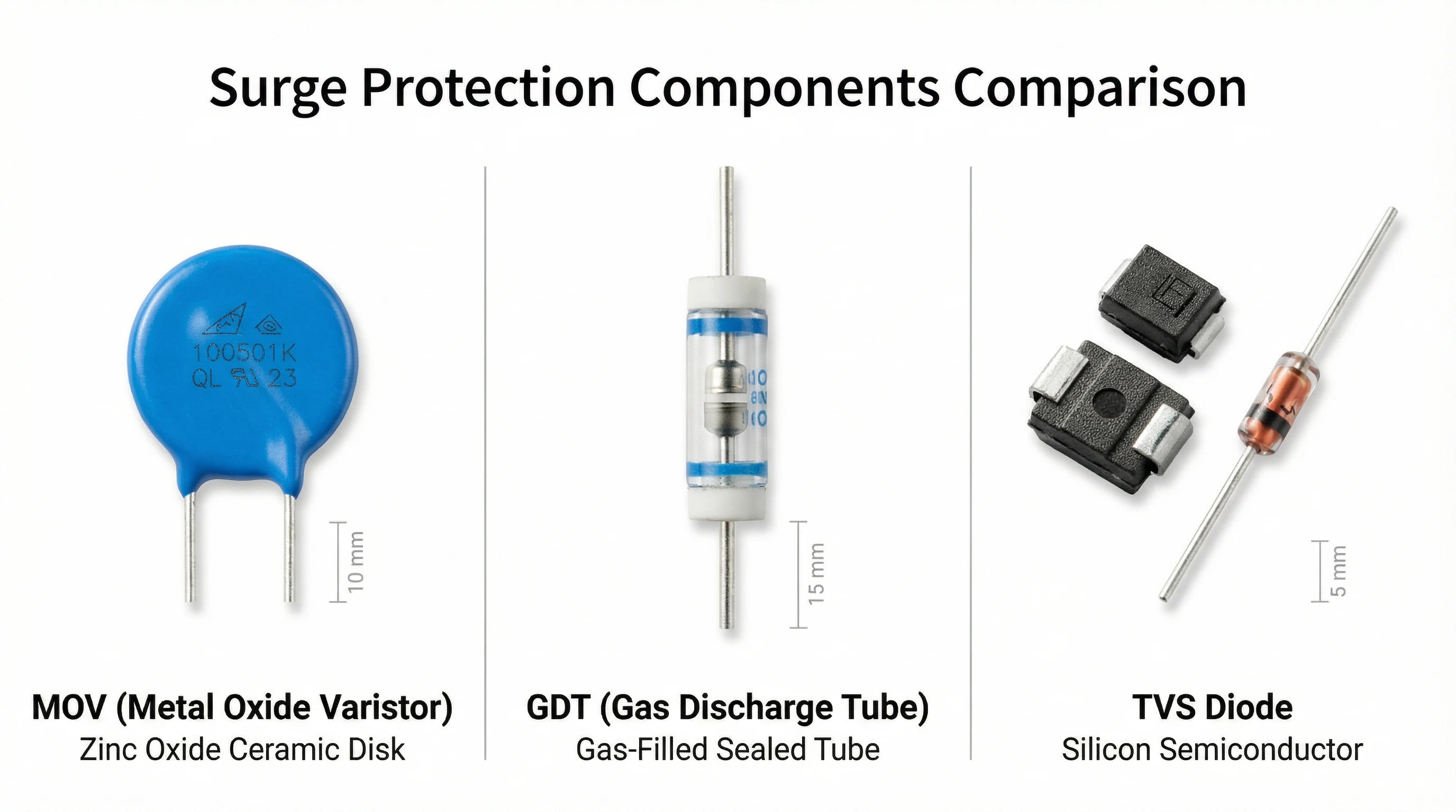
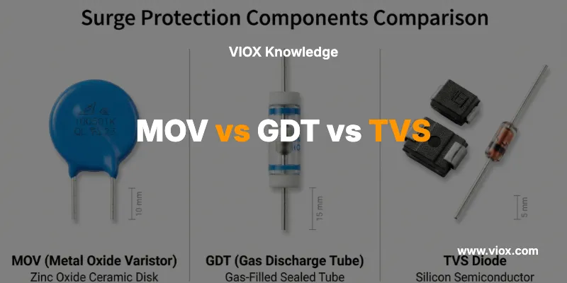
图0:三种浪涌防护技术的实物对比。左:MOV(金属氧化物压敏电阻)展示了标志性的蓝色氧化锌陶瓷圆盘与径向引线——其物理尺寸随额定电压(圆盘厚度)和通流能力(圆盘直径)而变化。中:GDT(气体放电管)呈现圆柱形密封玻璃/陶瓷外壳,内部充有惰性气体和电极——密闭结构确保稳定的火花放电特性。右:TVS二极管展示了从紧凑型贴片封装(0402、SOT-23)到较大通孔封装(DO-201、DO-218)等多种半导体封装形式——硅芯片尺寸决定脉冲功率额定值。这些显著的物理差异反映了根本不同的工作原理:陶瓷晶界结(MOV)、气体电离等离子体(GDT)以及半导体雪崩击穿(TVS)。.
MOV(金属氧化物压敏电阻):结构与工作原理
金属氧化物压敏电阻是一种陶瓷半导体器件,其电阻值随电压升高而急剧下降。这种压敏特性使其能够作为自动电压钳位器件——在浪涌期间大电流导通,而在正常工作时几乎处于隐形状态。.
内部结构
MOV由氧化锌(ZnO)晶粒烧结而成,并含有少量铋、钴、锰及其他金属氧化物。其关键作用发生在晶界处。相邻ZnO晶粒之间的每个界面都形成一个微观的肖特基势垒——本质上是一个微小的背对背二极管结。单个MOV圆片包含数百万个这样的微结,它们以复杂的三维串并联网络连接。.
器件的整体特性源于这种微观结构。圆片厚度决定工作电压(串联晶界越多 = 额定电压越高)。圆片直径决定电流能力(并联路径越多 = 浪涌电流越高)。因此MOV数据手册会规定每毫米厚度的压敏电压,这也是用于配电的高能MOV在物理上通常是大型块状或圆片组件的原因。.
လည်ပတ်မှုနိယာမ
在电压低于压敏电压(Vᵥ)时,晶界结保持耗尽模式,器件仅吸收微安级的漏电流。当浪涌使电压超过Vᵥ时,结通过量子隧穿和雪崩倍增效应击穿。电阻从兆欧级骤降至欧姆级,MOV将浪涌电流旁路至地。.
这种转变本质上是快速的——在材料层面为亚纳秒级。标准目录型MOV的响应时间低于25纳秒,其主要限制来自引线电感和封装结构,而非ZnO的物理特性。其电压-电流特性呈高度非线性,通常用公式 I = K·Vᵅ 描述,非线性系数α范围在25至50之间(线性电阻的α = 1)。.
关键规格与特性
能量处理能力:MOV擅长吸收浪涌能量。制造商采用2毫秒矩形脉冲标定能量承受能力,并使用标准8/20 µs波形标定浪涌电流。用于配电的块状MOV单次事件可处理10,000至100,000安培的浪涌电流。.
老化与退化:反复承受浪涌会导致累积的微观结构损伤。压敏电压下降,漏电流增加,钳位性能退化。严重过载可能击穿晶界,形成永久性导电路径。因此,数据手册会规定重复浪涌的降额系数,关键安装场合应将MOV漏电流作为维护参数进行监测。.
ပံုမွန္အသံုးခ်ျခင္း:交流电源浪涌保护、配电盘、工业电机驱动、重型设备以及任何需要高能量吸收和快速(纳秒级)响应的应用。.
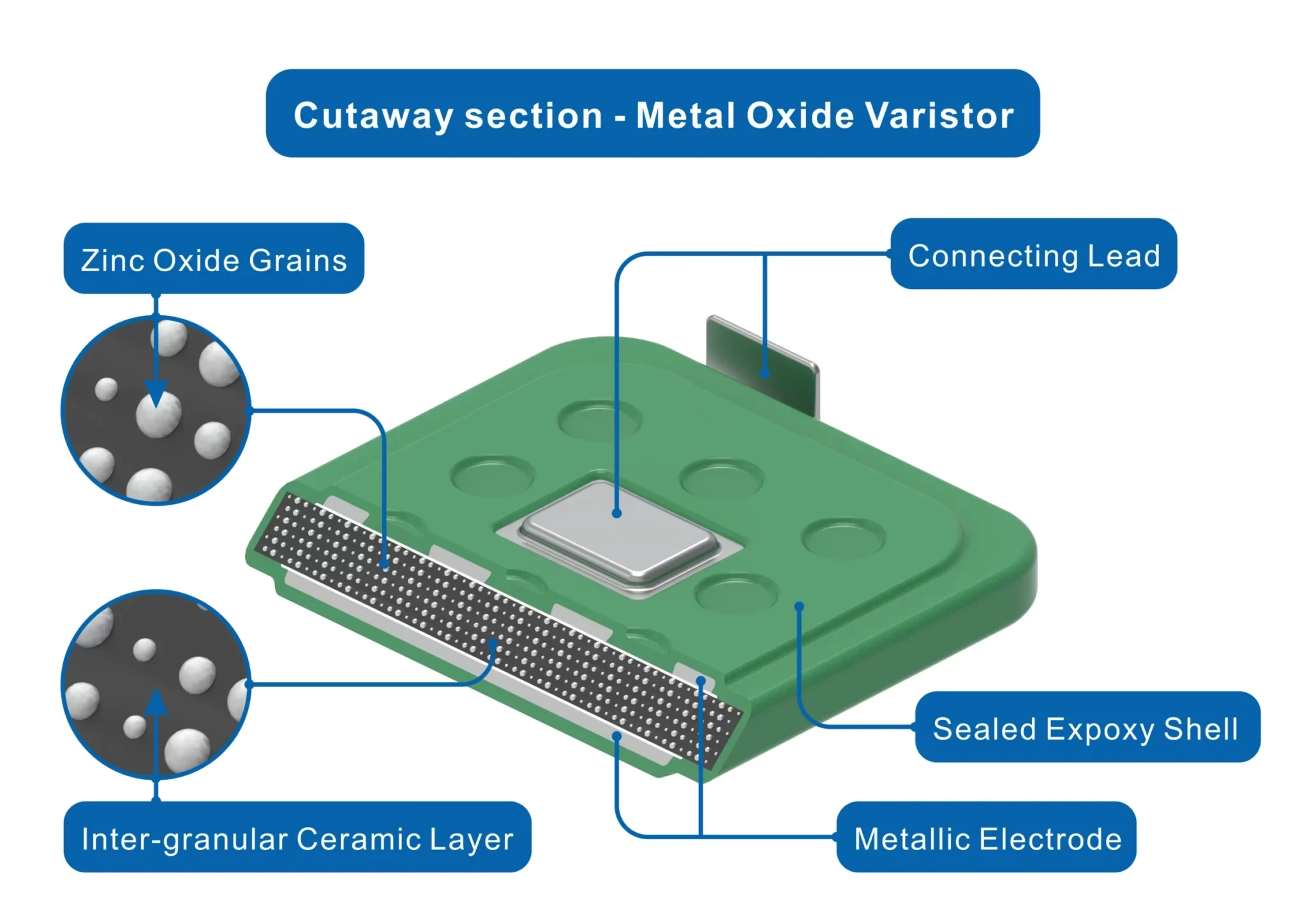
图1:MOV剖面图显示氧化锌(ZnO)晶粒嵌入陶瓷基体中,具有晶间边界(放大插图)。每个晶界形成一个微观肖特基势垒,构成数百万个串并联配置的微结。圆片的物理尺寸——厚度决定额定电压(串联边界越多),直径决定电流能力(并联路径越多)——直接控制浪涌保护性能。.
GDT(气体放电管):结构与工作原理
气体放电管采用根本不同的方法:它不是通过非线性电阻钳位电压,而是在电压超过阈值时形成临时短路。这种“撬杠”作用通过电离气体而非固态材料来泄放浪涌电流。.
内部结构
GDT由两个或三个电极组成,密封在充有惰性气体(通常是氩、氖或氙的混合气体,压力低于大气压)的陶瓷或玻璃外壳内。电极间隙和气体成分决定击穿电压。气密密封至关重要——任何污染或压力变化都会改变击穿特性。.
三电极GDT常见于电信应用,可在单个元件中提供线对线和线对地保护。双电极版本用于更简单的线对地配置。电极常涂覆有降低击穿电压和稳定电弧形成的材料。.
လည်ပတ်မှုနိယာမ
正常情况下,气体不导电,GDT呈现近乎无限的阻抗(>10⁹ Ω)和极低的电容——通常低于2皮法。当瞬态电压超过火花放电电压时,电场使气体电离。自由电子加速并与气体原子碰撞,在雪崩过程中释放更多电子。在微秒级时间内,电极间形成导电等离子体通道。.
一旦电离,GDT进入电弧模式。器件两端电压降至低电弧电压——通常为10-20伏,与初始击穿电压无关。此时器件近似短路,通过等离子体泄放浪涌电流。电弧持续至电流低于“辉光-电弧转换电流”(通常为数十毫安)为止。.
ဤ crowbar သဘောထားသည် အရေးကြီးသော ဒီဇိုင်းကို ထည့်သွင်းစဉ်းစားရန် လိုအပ်သည်- အကယ်၍ ကာကွယ်ထားသော ဆားကစ်သည် တောက်ပမှုအဆင့်ထက် လုံလောက်သော “နောက်ဆက်တွဲ လျှပ်စီးကြောင်း” ကို ထုတ်ပေးနိုင်ပါက၊ ယာယီဖြစ်ရပ် ပြီးဆုံးသွားပြီးနောက်တွင်ပင် GDT သည် လျှပ်ကူးမှုတွင် ဆက်လက်တည်ရှိနေနိုင်သည်။ AC mains ရှိ GDT များသည် စီးရီးခုခံမှု သို့မဟုတ် upstream breakers များနှင့် ညှိနှိုင်းမှု လိုအပ်ရခြင်း၏ အကြောင်းရင်းဖြစ်သည်။ impedance နည်းသော DC supply များတွင်၊ နောက်ဆက်တွဲ လျှပ်စီးကြောင်း ဆက်လက်တည်ရှိနေခြင်းသည် အလွန်ဆိုးရွားနိုင်သည်။.
关键规格与特性
Surge Current Capability (မြင့်မားသော လျှပ်စီးကြောင်း ခံနိုင်ရည်): GDT များသည် အလွန်မြင့်မားသော surge current များကို ကိုင်တွယ်နိုင်သည်—ပုံမှန် တယ်လီကွန်းအဆင့် စက်ပစ္စည်းများသည် 10,000 မှ 20,000 amperes (8/20 µs waveform) အထိ အဆင့်သတ်မှတ်ထားပြီး multi-shot ခံနိုင်ရည်ရှိသည်။ ဤမြင့်မားသော စွမ်းရည်သည် ဒေသအလိုက် solid-state junction များထက် plasma channel ၏ ဖြန့်ဝေထားသော သဘောသဘာဝမှ ရရှိလာခြင်းဖြစ်သည်။.
Capacitance (ကပ္ပစီတန့်): GDT များ၏ အဓိကအားသာချက်မှာ ၎င်းတို့၏ sub-2 pF capacitance ဖြစ်ပြီး၊ ၎င်းသည် မြန်နှုန်းမြင့် အချက်ပြမှုများအတွက် ပွင့်လင်းမြင်သာစေသည်။ ဤအကြောင်းကြောင့် ၎င်းတို့သည် တယ်လီကွန်းလိုင်း ကာကွယ်ရေးတွင် လွှမ်းမိုးထားခြင်းဖြစ်သည်- xDSL၊ cable broadband နှင့် Gigabit Ethernet တို့သည် MOV များ သို့မဟုတ် TVS စက်ပစ္စည်းများစွာ၏ capacitance ကို ခံနိုင်ရည်မရှိပါ။.
တုန့်ပြန်အချိန်: GDT များသည် solid-state စက်ပစ္စည်းများထက် နှေးကွေးသည်။ Breakdown သည် ပုံမှန်အားဖြင့် nanosecond ရာဂဏန်းမှ microsecond အနည်းငယ်အတွင်း ဖြစ်ပေါ်ပြီး ဗို့အား overshoot ပေါ်မူတည်သည် (မြင့်မားသော dV/dt သည် ionization ကို အရှိန်မြှင့်ပေးသည်)။ အထိခိုက်မခံသော အီလက်ထရွန်းနစ်ပစ္စည်းများပေါ်ရှိ မြန်ဆန်သော ယာယီဖြစ်ရပ်များအတွက်၊ GDT များကို ညှိနှိုင်းထားသော ကာကွယ်ရေးအစီအစဉ်တွင် ပိုမိုမြန်ဆန်သော clamp များနှင့် တွဲဖက်အသုံးပြုလေ့ရှိသည်။.
Stability and Lifespan (တည်ငြိမ်မှုနှင့် သက်တမ်း): အရည်အသွေးကောင်းမွန်သော GDT များသည် ရေရှည်တည်ငြိမ်မှုကို ပြသသည်။ ITU-T K.12 နှင့် IEEE C62.31 စမ်းသပ်နည်းလမ်းများသည် surge cycle ထောင်ပေါင်းများစွာကျော်တွင် စွမ်းဆောင်ရည်ကို အတည်ပြုသည်။ UL မှ အသိအမှတ်ပြုထားသော တယ်လီကွန်း GDT များသည် ဆယ်စုနှစ်များစွာ ဝန်ဆောင်မှုပေးရာတွင် parameter အနည်းငယ်သာ ပြောင်းလဲကြောင်း သက်သေပြသည်။.
ပံုမွန္အသံုးခ်ျခင္း: တယ်လီကွန်းလိုင်း ကာကွယ်ရေး (xDSL, cable, fiber optics), မြန်နှုန်းမြင့် Ethernet interfaces, RF နှင့် antenna inputs နှင့် လိုင်းတင်မှု အနည်းဆုံးဖြစ်ရန် လိုအပ်ပြီး surge source impedance သည် နောက်ဆက်တွဲ လျှပ်စီးကြောင်း ဆက်လက်တည်ရှိနေခြင်းကို ကာကွယ်ရန် လုံလောက်သော မည်သည့် application မဆို။.
ပုံ ၂- Gas Discharge Tube (GDT) တည်ဆောက်ပုံနှင့် လည်ပတ်မှုပုံစံ။ ဘယ်ဘက်ပုံတွင် အတွင်းပိုင်းဖွဲ့စည်းပုံကို ပြသထားသည်- electrode gap နှင့် inert gas fill (argon/neon) ပါသော hermetically sealed gas chamber။ ညာဘက်ဂရပ်သည် ionization တုံ့ပြန်မှုကို သရုပ်ဖော်သည်—ယာယီဗို့အားသည် spark-over threshold ထက်ကျော်လွန်သောအခါ၊ ဓာတ်ငွေ့သည် conductive plasma channel ကို ဖန်တီးပေးပြီး၊ ဗို့အားသည် arc mode (~10-20V) သို့ ကျဆင်းသွားပြီး လျှပ်စီးကြောင်းသည် glow-to-arc transition threshold အောက်သို့ ကျဆင်းသွားသည်အထိ plasma မှတဆင့် လမ်းကြောင်းပြောင်းသွားသည်။.
TVS Diode: Structure and Operating Principle (TVS ဒိုင်အုတ်- ဖွဲ့စည်းပုံနှင့် လည်ပတ်မှုနိယာမ)
Transient Voltage Suppressor ဒိုင်အုတ်များသည် surge clamping အတွက် အထူးထုတ်လုပ်ထားသော ဆီလီကွန် avalanche စက်ပစ္စည်းများဖြစ်သည်။ ၎င်းတို့သည် အထိခိုက်မခံသော ဆီမီးကွန်ဒတ်တာ ဆားကစ်များကို ကာကွယ်ရန်အတွက် ဦးစားပေးရွေးချယ်မှုဖြစ်စေသော surge protection အစိတ်အပိုင်းများတွင် ရရှိနိုင်သော အမြန်ဆုံးတုံ့ပြန်မှုအချိန်များနှင့် အနိမ့်ဆုံး clamping ဗို့အားများကို ပေါင်းစပ်ထားသည်။.
内部结构
TVS ဒိုင်အုတ်သည် ဗို့အားထိန်းညှိခြင်းထက် မြင့်မားသော pulse power အတွက် အကောင်းဆုံးဖြစ်အောင် ပြုလုပ်ထားသော အထူးပြု Zener ဒိုင်အုတ်ဖြစ်သည်။ ဆီလီကွန် die သည် တိကျသောဗို့အားတွင် avalanche breakdown သို့ ဝင်ရောက်ရန် ဒီဇိုင်းထုတ်ထားသော အလွန်အမင်း doped P-N junction ကို ပါရှိသည်။ Die ဧရိယာသည် surge ဖြစ်ရပ်များ၏ peak current များကို ကိုင်တွယ်ရန်အတွက် ညီမျှသော Zener regulators များထက် များစွာကြီးမားသည်—submicrosecond pulses များတွင် ရာဂဏန်း amperes များ။.
လည်ပတ်မှုနိယာမ
ပုံမှန်လည်ပတ်ဗို့အားအောက်တွင်၊ TVS ဒိုင်အုတ်သည် nanoampere-level leakage ဖြင့် reverse bias တွင် လည်ပတ်သည်။ ယာယီဖြစ်ရပ်သည် reverse breakdown voltage (V_BR) ထက်ကျော်လွန်သောအခါ၊ ဆီလီကွန် junction သည် avalanche multiplication သို့ ဝင်ရောက်သည်။ Impact ionization သည် electron-hole pairs များကို ရေလွှမ်းမိုးစေပြီး junction resistance သည် ပြိုလဲသွားသည်။ စက်ပစ္စည်းသည် breakdown အဆင့်တွင် ဗို့အားကို clamp လုပ်ပြီး dynamic resistance သည် surge current နှင့် မြှောက်ထားသည်။.
ရူပဗေဒသည် စက်ပိုင်းဆိုင်ရာ လှုပ်ရှားမှု၊ ဓာတ်ငွေ့ ionization သို့မဟုတ် ပစ္စည်းအဆင့် ပြောင်းလဲခြင်းမရှိသော သက်သက် solid-state ဖြစ်သည်။ ၎င်းသည် nanosecond အပိုင်းအခြားအတွင်း တုံ့ပြန်မှုအချိန်များကို ဖွင့်ပေးသည်—အဝတ်မပါသော ဆီလီကွန်အတွက် sub-1 ns ဖြစ်သော်လည်း package inductance သည် လက်တွေ့စက်ပစ္စည်းများအတွက် ထိရောက်သော တုံ့ပြန်မှုကို 1-5 ns သို့ တွန်းပို့လေ့ရှိသည်။ ဗို့အား-လျှပ်စီးကြောင်း လက္ခဏာသည် အလွန်မတ်စောက်သည် (dynamic resistance နည်းပါးသည်)၊ တင်းကျပ်သော clamping ကို ပေးစွမ်းသည်။.
关键规格与特性
Pulse Power Ratings (Pulse Power အဆင့်သတ်မှတ်ချက်များ): TVS ထုတ်လုပ်သူများသည် စံသတ်မှတ်ထားသော pulse widths (ပုံမှန်အားဖြင့် 10/1000 µs exponential waveforms) ကို အသုံးပြု၍ power capacity ကို သတ်မှတ်သည်။ ဘုံထုတ်ကုန်မိသားစုများသည် 400W, 600W, 1500W သို့မဟုတ် 5000W pulse ratings ကို ပေးဆောင်သည်။ Peak current capability ကို pulse power နှင့် clamping voltage မှ တွက်ချက်သည်—15V clamp ပါသော 600W စက်ပစ္စည်းသည် 40A peak ခန့်ကို ကိုင်တွယ်နိုင်သည်။.
Clamping Performance (Clamping စွမ်းဆောင်ရည်): TVS ဒိုင်အုတ်များသည် မည်သည့် surge protection နည်းပညာထက်မဆို အနိမ့်ဆုံး clamping ဗို့အားများကို ပေးဆောင်သည်။ Clamping voltage နှင့် standoff voltage (V_C/V_WM) အချိုးသည် ပုံမှန်အားဖြင့် 1.3 မှ 1.5 ဖြစ်ပြီး MOV များအတွက် 2.0-2.5 နှင့် နှိုင်းယှဉ်နိုင်သည်။ ဤတင်းကျပ်သော ထိန်းချုပ်မှုသည် 3.3V logic, 5V USB, 12V automotive circuits နှင့် အခြားဗို့အား အထိခိုက်မခံသော load များကို ကာကွယ်ရန်အတွက် အရေးကြီးပါသည်။.
Capacitance (ကပ္ပစီတန့်): TVS capacitance သည် စက်ပစ္စည်း တည်ဆောက်မှုနှင့်အတူ ကျယ်ပြန့်စွာ ကွဲပြားသည်။ စံ junction TVS ဒိုင်အုတ်များသည် picofarad ရာဂဏန်းများကို ပြသနိုင်ပြီး၊ ၎င်းသည် မြန်နှုန်းမြင့် ဒေတာလိုင်းများကို တင်ဆောင်သည်။ HDMI, USB 3.0, Ethernet နှင့် RF အတွက် အင်ဂျင်နီယာလုပ်ထားသော Low-capacitance TVS မိသားစုများသည် အထူးပြု junction geometries ကို အသုံးပြုပြီး တစ်လိုင်းလျှင် sub-5 pF ကို ရရှိသည်။.
Aging and Reliability (အိုမင်းခြင်းနှင့် ယုံကြည်စိတ်ချရမှု): MOV များမတူဘဲ၊ TVS ဒိုင်အုတ်များသည် အဆင့်သတ်မှတ်ထားသော pulse stress အောက်တွင် စွမ်းဆောင်ရည် အနည်းငယ်သာ ပြောင်းလဲမှုကို ပြသသည်။ ဆီလီကွန် junction သည် အဆင့်သတ်မှတ်ချက်အတွင်း ထပ်ခါထပ်ခါ surge များမှ စုပုံ၍ ယိုယွင်းခြင်းမရှိပါ။ Failure modes များသည် ပုံမှန်အားဖြင့် open-circuit (junction annihilation) သို့မဟုတ် short-circuit (metallization fusing) ဖြစ်ပြီး၊ ၎င်းနှစ်ခုစလုံးသည် အဆင့်သတ်မှတ်ချက်ထက် ကျော်လွန်သော အလွန်အမင်း overload အောက်တွင်သာ ဖြစ်ပေါ်သည်။.
ပံုမွန္အသံုးခ်ျခင္း: Board-level circuit protection (I/O ports, power rails), USB နှင့် HDMI interfaces, automotive electronics, DC power supplies, communication data lines နှင့် ဆီမီးကွန်ဒတ်တာ load များအတွက် မြန်ဆန်သော တုံ့ပြန်မှုနှင့် တင်းကျပ်သော ဗို့အား clamping လိုအပ်သော မည်သည့် application မဆို။.
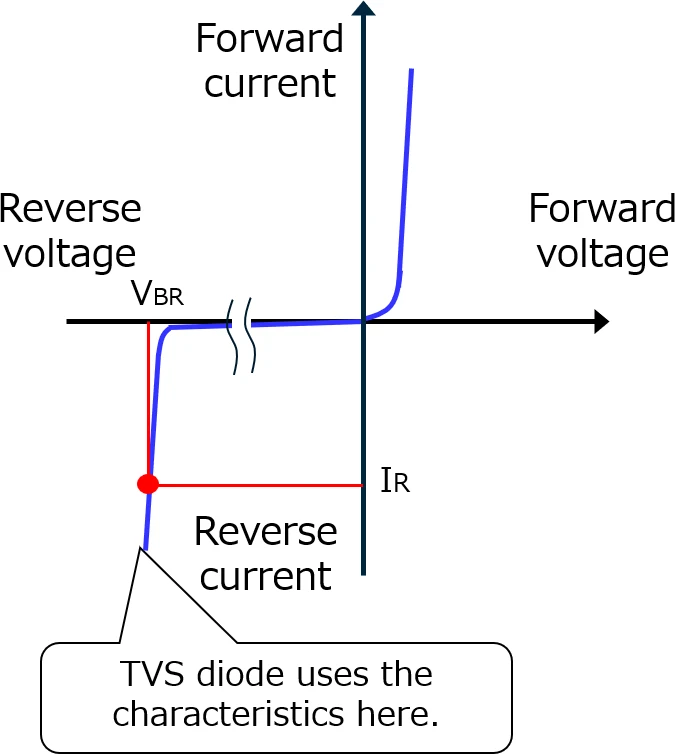
ပုံ ၃- ဆီမီးကွန်ဒတ်တာ avalanche လည်ပတ်မှုကို ပြသထားသော TVS ဒိုင်အုတ် ဗို့အား-လျှပ်စီးကြောင်း (I-V) လက္ခဏာမျဉ်း။ ပုံမှန်ဗို့အား (V_WM standoff region) အောက်တွင်၊ စက်ပစ္စည်းသည် nanoampere leakage ဖြင့် မြင့်မားသော impedance ကို ထိန်းသိမ်းထားသည်။ ယာယီဖြစ်ရပ်သည် reverse breakdown voltage (V_BR) ထက်ကျော်လွန်သောအခါ၊ ဆီလီကွန် P-N junction သည် avalanche multiplication သို့ ဝင်ရောက်သည်—junction resistance သည် ပြိုလဲသွားပြီး စက်ပစ္စည်းသည် V_C တွင် ဗို့အားကို clamp လုပ်သည် (breakdown voltage plus dynamic resistance × surge current)။ မတ်စောက်သော မျဉ်းကွေး (dynamic resistance နည်းပါးသည်) သည် ဆီမီးကွန်ဒတ်တာ load များကို ကာကွယ်ရန်အတွက် အရေးကြီးသော တင်းကျပ်သော ဗို့အား ထိန်းချုပ်မှုကို ပေးစွမ်းသည်။.
Clamping vs Crowbar: Two Protection Philosophies (Clamping နှင့် Crowbar- ကာကွယ်ရေး အတွေးအခေါ် နှစ်ခု)
ဤနည်းပညာများကြား အခြေခံကွာခြားချက်မှာ ၎င်းတို့၏ ကာကွယ်ရေး အတွေးအခေါ်တွင် တည်ရှိသည်။ MOV များနှင့် TVS ဒိုင်အုတ်များသည် clamping devices (ဗို့အားကို ထိန်းညှိပေးသော စက်များ)—၎င်းတို့သည် surge current နှင့် အချိုးကျသော သီးခြားအဆင့်တစ်ခုအထိ ဗို့အားကို ကန့်သတ်ထားသည်။ GDT များသည် crowbar devices (လျှပ်စီးကြောင်းကို ဖြတ်တောက်ပေးသော စက်များ)—၎င်းတို့သည် လျှပ်စီးကြောင်း ပမာဏ မည်သို့ပင်ရှိစေကာမူ ဗို့အားကို အနိမ့်ဆုံးကျန်ရှိသော အဆင့်သို့ ပြိုလဲစေသော short circuit ကို ဖန်တီးပေးသည်။.
Clamping behavior (Clamping အပြုအမူ) (MOV နှင့် TVS): surge current တိုးလာသည်နှင့်အမျှ clamping voltage သည် စက်ပစ္စည်း၏ nonlinear V-I မျဉ်းကွေးအရ မြင့်တက်လာသည်။ 275V RMS အဆင့်သတ်မှတ်ထားသော MOV သည် 1 kA surge အတွက် 750V တွင် clamp လုပ်နိုင်သော်လည်း 5 kA တွင် 900V သို့ မြင့်တက်နိုင်သည်။ 15V standoff အဆင့်သတ်မှတ်ထားသော TVS ဒိုင်အုတ်သည် 10A အတွက် 24V တွင် clamp လုပ်နိုင်သော်လည်း 20A တွင် 26V သို့ ရောက်ရှိနိုင်သည်။ ကာကွယ်ထားသော load သည် surge amplitude နှင့် စက်ပစ္စည်း လက္ခဏာများဖြင့် ဆုံးဖြတ်ထားသော ဗို့အားကို မြင်တွေ့ရသည်။.
Crowbar behavior (Crowbar အပြုအမူ) (GDT): breakdown ဖြစ်ပေါ်ပြီးသည်နှင့် GDT သည် arc mode သို့ ဝင်ရောက်ပြီး surge current သည် 100A သို့မဟုတ် 10,000A ဖြစ်စေကာမူ ဗို့အားသည် 10-20V သို့ ပြိုလဲသွားသည်။ ၎င်းသည် trigger လုပ်ပြီးသည်နှင့် ကောင်းမွန်သော ကာကွယ်မှုကို ပေးစွမ်းသော်လည်း initial spark-over သည် ionization မပြီးဆုံးမီ ဗို့အား spike ကို ခွင့်ပြုနိုင်သည်။ ဤအကြောင်းကြောင့် GDT များနောက်ကွယ်ရှိ အထိခိုက်မခံသော load များသည် ဒုတိယမြန်ဆန်သော clamp လိုအပ်လေ့ရှိသည်။.
အတွေးအခေါ်တစ်ခုစီသည် မတူညီသော application များနှင့် သင့်လျော်သည်။ Clamping စက်များသည် ဗို့အားထိတွေ့မှုကို ကန့်သတ်ခြင်းဖြင့် ကာကွယ်ပေးသည်။ Crowbar စက်များသည် လျှပ်စီးကြောင်းကို လမ်းကြောင်းပြောင်းခြင်းဖြင့် ကာကွယ်ပေးသည်။ Clamping သည် ကာကွယ်ထားသော ဆားကစ်သည် clamp voltage ကို ခံနိုင်ရည်ရှိသောအခါ အလုပ်လုပ်သည်။ Crowbar သည် surge source တွင် လိုင်းကို short လုပ်ခြင်းသည် upstream ပစ္စည်းများကို မပျက်စီးစေဘဲ သို့မဟုတ် နောက်ဆက်တွဲ လျှပ်စီးကြောင်း ပြဿနာများကို မဖြစ်စေရန် လုံလောက်သော impedance မြင့်မားသောအခါ အလုပ်လုပ်သည်။.
MOV vs GDT vs TVS: Side-by-Side Comparison (MOV နှင့် GDT နှင့် TVS- ဘေးချင်းယှဉ် နှိုင်းယှဉ်ခြင်း)
အောက်ဖော်ပြပါ ဇယားသည် ဤ surge protection နည်းပညာသုံးခုကြားရှိ အဓိက စွမ်းဆောင်ရည် ကွာခြားချက်များကို ပမာဏအလိုက် ဖော်ပြထားသည်-
| ဇာတိ | MOV (Metal Oxide Varistor) | GDT (Gas Discharge Tube) | ဗီြႏွင့္ဗီြဒီ Diode |
| လည်ပတ်မှုနိယာမ | Voltage-dependent nonlinear resistance (ZnO grain boundaries) (ဗို့အားပေါ်မူတည်သော nonlinear ခုခံမှု (ZnO grain boundaries)) | Gas ionization crowbar (ဓာတ်ငွေ့ ionization လျှပ်စီးကြောင်း ဖြတ်တောက်ခြင်း) | Semiconductor avalanche breakdown (ဆီမီးကွန်ဒတ်တာ avalanche ပြိုလဲခြင်း) |
| ကာကွယ်မှု ယန္တရား | Clamping (ဗို့အားကို ထိန်းညှိပေးခြင်း) | Crowbar (လျှပ်စီးကြောင်းကို ဖြတ်တောက်ခြင်း) | Clamping (ဗို့အားကို ထိန်းညှိပေးခြင်း) |
| တုန့်ပြန်အချိန် | <25 ns (ပုံမှန် catalog အစိတ်အပိုင်းများ) | 100 ns – 1 µs (ဗို့အားပေါ်မူတည်သည်) | 1-5 ns (package-limited) |
| Clamping/Arc Voltage (Clamping/Arc ဗို့အား) | 2.0-2.5 × MCOV | 10-20 V (arc mode) | 1.3-1.5 × V_standoff |
| Surge Current (8/20 µs) (မြင့်မားသော လျှပ်စီးကြောင်း (8/20 µs)) | 400 A – 100 kA (အရွယ်အစားပေါ်မူတည်သည်) | 5 kA – 20 kA (တယ်လီကွန်းအဆင့်) | 10 A – 200 A (600W မိသားစု ~40A) |
| 能量处理能力 | Excellent (100-1000 J) (အလွန်ကောင်းမွန်သည် (100-1000 J)) | Excellent (distributed plasma) (အလွန်ကောင်းမွန်သည် (ဖြန့်ဝေထားသော plasma)) | Moderate (limited by junction) (အသင့်အတင့် (junction ဖြင့် ကန့်သတ်ထားသည်)) |
| Capacitance (ကပ္ပစီတန့်) | 50-5000 pF (ဧရိယာပေါ်မူတည်သည်) | <2 pF | 5-500 pF (တည်ဆောက်မှုပေါ်မူတည်သည်) |
| Aging Behavior (အိုမင်းခြင်း အပြုအမူ) | Degrades with surge cycles; V_n drifts down (surge cycle များဖြင့် ယိုယွင်းလာသည်; V_n သည် အောက်သို့ ရွေ့လျားသည်) | Stable over thousands of surges (surge ထောင်ပေါင်းများစွာကျော်တွင် တည်ငြိမ်သည်) | သတ်မှတ်ချက်အတွင်း အနည်းဆုံး မျောပါမှု |
| ပျက်ကွက်မှုပုံစံ | ယိုယွင်းပျက်စီးခြင်း → ဝါယာရှော့ (သို့) ပွင့်သွားခြင်း | ဝါယာရှော့ (လျှပ်စစ်မီးပွား ထိန်းထားနိုင်ခြင်း) | ပွင့်သွားခြင်း (သို့) ဝါယာရှော့ (အကြီးအကျယ် ပျက်စီးခြင်းသာ) |
| နောက်ဆက်တွဲ လျှပ်စီးကြောင်းအန္တရာယ် | နည်းပါးခြင်း (အလိုအလျောက် ငြိမ်းသတ်နိုင်ခြင်း) | မြင့်မားခြင်း (ပြင်ပကန့်သတ်ချက် လိုအပ်ခြင်း) | မရှိခြင်း (Solid-state) |
| ပုံမှန် ဗို့အားအကွာအဝေး | 18V RMS – 1000V RMS | 75V – 5000V DC sparkover | 3.3V – 600V standoff |
| ကုန်ကျစရိတ် (နှိုင်းယှဉ်) | နည်းပါးခြင်း ($0.10 – $5) | နည်းပါး-အလယ်အလတ် ($0.50 – $10) | နည်းပါး-အလယ်အလတ် ($0.20 – $8) |
| စံနှုန်းများ | IEC 61643-11, UL 1449 | ITU-T K.12, IEEE C62.31 | IEC 61643-11, UL 1449 |
| မူလတန်းကေးရှင်း | AC mains, power distribution, စက်မှုလုပ်ငန်း | Telecom lines, high-speed data, antenna | Board-level I/O, DC supplies, မော်တော်ကား |
နှိုင်းယှဉ်မှုမှ အဓိကရရှိသော အချက်များ
MOVs စွမ်းအင်ကိုင်တွယ်မှု၊ မြန်ဆန်သော တုံ့ပြန်မှုနှင့် ပါဝါအဆင့်မြင့် လျှပ်စီးကြောင်းများအတွက် ကုန်ကျစရိတ်တို့၏ အကောင်းဆုံး မျှတမှုကို ပေးသည်။ ၎င်းတို့သည် AC mains ကာကွယ်မှုတွင် လွှမ်းမိုးထားသော်လည်း ကြိမ်နှုန်းမြင့် ဆားကစ်များနှင့် ထပ်ခါတလဲလဲ ဖိစီးမှုအောက်တွင် စုပုံလာသော သက်တမ်းရင့်မှုများကြောင့် ခံစားရသည်။.
GDTs လိုင်းအားနည်းခြင်းသည် အရေးကြီးပြီး လျှပ်စီးကြောင်း စွမ်းရည်ကို အမြင့်ဆုံးမြှင့်တင်ရမည့်နေရာတွင် ထူးချွန်သည်။ ၎င်းတို့၏ အလွန်နည်းပါးသော Capacitance သည် တယ်လီကွန်းနှင့် RF အသုံးချမှုများတွင် အစားထိုး၍မရနိုင်သော်လည်း နှေးကွေးသော တုံ့ပြန်မှုနှင့် နောက်ဆက်တွဲ လျှပ်စီးကြောင်းအန္တရာယ်သည် ဂရုတစိုက် ဆားကစ်ဒီဇိုင်း လိုအပ်သည်။.
TVS diodes အထိခိုက်မခံသော အီလက်ထရွန်းနစ်ပစ္စည်းများအတွက် အမြန်ဆုံး၊ အတင်းကျပ်ဆုံး ညှပ်ခြင်းကို ပေးသည်။ ၎င်းတို့သည် 50V အောက် ဗို့အားများတွင် ဆီမီးကွန်ဒတ်တာ I/O ကို ကာကွယ်ရန်အတွက် လက်တွေ့ကျသော ရွေးချယ်မှုတစ်ခုသာဖြစ်သော်လည်း စွမ်းအင်ပမာဏ အကန့်အသတ်ရှိခြင်းကြောင့် MOVs နှင့် GDTs များ ပုံမှန်စုပ်ယူနိုင်သော လျှပ်စီးကြောင်းအဆင့်ကို မကိုင်တွယ်နိုင်ပါ။.
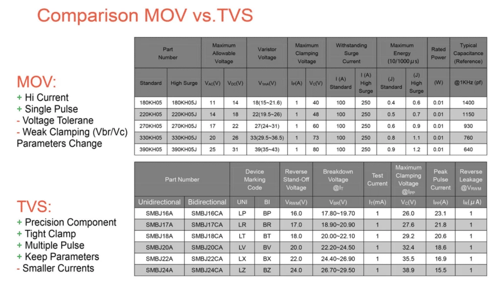
ပုံ ၄- အဓိက သတ်မှတ်ချက်များတွင် MOV (Metal Oxide Varistor) နှင့် TVS (Transient Voltage Suppressor) နည်းပညာများကို နှိုင်းယှဉ်ထားသော ပရော်ဖက်ရှင်နယ် နှိုင်းယှဉ်ဇယား။ MOVs များသည် ပါဝါအဆင့်မြင့် လျှပ်စီးကြောင်းများအတွက် အလွန်ကောင်းမွန်သော စွမ်းအင်စုပ်ယူမှုနှင့်အတူ မြင့်မားသော ညှပ်ဗို့အားအချိုး (2.0-2.5× MCOV) ကို ပြသထားပြီး TVS diodes များသည် ဆီမီးကွန်ဒတ်တာ ကာကွယ်မှုအတွက် ပိုမိုမြန်ဆန်သော တုံ့ပြန်မှု (<5 ns) ဖြင့် တင်းကျပ်သော ဗို့အားထိန်းချုပ်မှု (1.3-1.5× standoff) ကို ပေးသည်။ ဇယားတွင် ဗို့အားအဆင့်သတ်မှတ်ချက်များ၊ လျှပ်စီးကြောင်း စွမ်းရည်များနှင့် နည်းပညာတစ်ခုစီ၏ ဖြည့်စွက်စွမ်းဆောင်ရည်ကို သရုပ်ပြသော ပုံမှန်အစိတ်အပိုင်း နံပါတ် ဥပမာများ ပါဝင်သည်။.
နည်းပညာရွေးချယ်မှု လမ်းညွှန်- တစ်ခုစီကို ဘယ်အချိန်မှာ အသုံးပြုမလဲ
မှန်ကန်သော လျှပ်စီးကြောင်း ကာကွယ်ရေးနည်းပညာကို ရွေးချယ်ခြင်းသည် စက်ပစ္စည်း၏ လက္ခဏာများနှင့် ဆားကစ်လိုအပ်ချက်များနှင့် ကိုက်ညီမှုအပေါ် မူတည်ပါသည်။ ဤတွင် ဆုံးဖြတ်ချက်မူဘောင်တစ်ခုဖြစ်သည်။
MOV ကို အောက်ပါအခြေအနေများတွင် အသုံးပြုပါ-
- ဆားကစ်ဗို့အားသည် AC mains သို့မဟုတ် ဗို့အားမြင့် DC (>50V) ဖြစ်သည်။: MOVs များသည် 18V RMS မှ 1000V ကျော်အထိ ဗို့အားအဆင့်သတ်မှတ်ချက်များဖြင့် ရရှိနိုင်ပြီး လူနေအိမ် (120/240V)၊ စီးပွားဖြစ် (277/480V) နှင့် စက်မှုလုပ်ငန်း ပါဝါဖြန့်ဖြူးမှုများနှင့် လုံးဝကိုက်ညီပါသည်။.
- လျှပ်စီးကြောင်း စွမ်းအင် မြင့်မားသည်။: လျှပ်စီးကြောင်းကြောင့်ဖြစ်သော လျှပ်စီးကြောင်းများ၊ အသုံးအဆောင်ပစ္စည်းများ ပြောင်းလဲခြင်းနှင့် မော်တာများ စတင်လည်ပတ်ခြင်းတို့သည် MOVs များသာ စီးပွားရေးအရ စုပ်ယူနိုင်သော စွမ်းအင်အဆင့်များ (ဂျူးလ်ရာပေါင်းများစွာမှ ထောင်ပေါင်းများစွာ) ကို ထုတ်လုပ်ပေးသည်။.
- တုံ့ပြန်ချိန် <25 ns သည် လက်ခံနိုင်ဖွယ်ရှိသည်။: ပါဝါအီလက်ထရွန်းနစ်နှင့် စက်မှုပစ္စည်းအများစုသည် MOV တုံ့ပြန်မှုအမြန်နှုန်းကို ခံနိုင်ရည်ရှိသည်။.
- Capacitance တင်ခြင်းကို လက်ခံနိုင်ဖွယ်ရှိသည်။: ပါဝါကြိမ်နှုန်းများ (50/60 Hz) တွင်ပင် 1000 pF capacitance သည် အရေးမပါပါ။.
- ကုန်ကျစရိတ် ကန့်သတ်ထားသည်။: MOVs များသည် ကာကွယ်မှု၏ ဂျူးလ်တစ်ခုလျှင် အနိမ့်ဆုံးကုန်ကျစရိတ်ကို ပေးသည်။.
MOVs များကို အောက်ပါအခြေအနေများတွင် ရှောင်ကြဉ်ပါ မြန်နှုန်းမြင့် ဆက်သွယ်ရေးလိုင်းများ (capacitance တင်ခြင်း)၊ ဗို့အားနည်း ဆီမီးကွန်ဒတ်တာ ဆားကစ်များ (ညှပ်ဗို့အား မြင့်လွန်းခြင်း) သို့မဟုတ် ဆယ်စုနှစ်များအတွင်း မည်သည့်မျောပါမှုမှ မရှိစေရန် အာမခံထားသော အသုံးချမှုများ (သက်တမ်းရင့်မှု စိုးရိမ်မှုများ) ကို ကာကွယ်ပါ။.
GDT ကို အောက်ပါအခြေအနေများတွင် အသုံးပြုပါ-
- လိုင်းတင်ခြင်းသည် အနည်းဆုံး (<2 pF) ဖြစ်ရမည်။: xDSL modem များ၊ cable broadband၊ Gigabit Ethernet၊ RF receivers နှင့် antenna inputs များသည် MOVs သို့မဟုတ် standard TVS စက်ပစ္စည်းများ၏ capacitance ကို ခံနိုင်ရည်မရှိပါ။.
- လျှပ်စီးကြောင်း စွမ်းရည်ကို အမြင့်ဆုံးမြှင့်တင်ရမည်။: တယ်လီကွန်းဗဟိုရုံးများ၊ ဆဲလ်တာဝါများနှင့် ပြင်ပတပ်ဆင်မှုများသည် TVS အဆင့်သတ်မှတ်ချက်ထက် ကျော်လွန်သော ထပ်ခါတလဲလဲ မြင့်မားသော လျှပ်စီးကြောင်းများကို ရင်ဆိုင်ရသည်။.
- ကာကွယ်ထားသော ဆားကစ်တွင် မြင့်မားသော source impedance ရှိသည်။: တယ်လီဖုန်းလိုင်းများ (600Ω)၊ antenna feedlines (50-75Ω) နှင့် data cable များကို အလွန်အကျွံ နောက်ဆက်တွဲ လျှပ်စီးကြောင်းမရှိဘဲ ဘေးကင်းစွာ crowbarred ပြုလုပ်နိုင်သည်။.
- လည်ပတ်ဗို့အား မြင့်မားသည် (>100V): GDTs များသည် 75V မှ 5000V အထိ sparkover ဗို့အားများဖြင့် ရရှိနိုင်ပြီး တယ်လီကွန်းဗို့အားများ၊ PoE (Power over Ethernet) နှင့် ဗို့အားမြင့် အချက်ပြခြင်းတို့ကို အကျုံးဝင်ပါသည်။.
GDTs များကို အောက်ပါအခြေအနေများတွင် ရှောင်ကြဉ်ပါ impedance နည်းသော DC ပါဝါထောက်ပံ့မှုများ (နောက်ဆက်တွဲ လျှပ်စီးကြောင်းအန္တရာယ်)၊ အမြန်ဆုံးတုံ့ပြန်မှု လိုအပ်သော ဆားကစ်များ (<100 ns အရေးကြီးသည်) သို့မဟုတ် မူလ spark-over spike ကို ခံနိုင်ရည်မရှိသော ဗို့အားထိခိုက်လွယ်သော ဝန်များ (ဒုတိယ ညှပ်ခြင်း လိုအပ်သည်) ကို ကာကွယ်ပါ။.
TVS Diode ကို အောက်ပါအခြေအနေများတွင် အသုံးပြုပါ-
- ညှပ်ဗို့အားကို တင်းကျပ်စွာ ထိန်းချုပ်ရမည်။: 3.3V logic, 5V USB, 12V မော်တော်ကား ဆားကစ်များနှင့် အခြား ဆီမီးကွန်ဒတ်တာ ဝန်များသည် ပုံမှန်ဗို့အား၏ 20-30% အတွင်း ညှပ်ရန်လိုအပ်သည်—TVS diodes များသာ ဤအရာကို ပေးစွမ်းနိုင်သည်။.
- တုံ့ပြန်ချိန်သည် အမြန်ဆုံးဖြစ်ရမည် (<5 ns): မြန်နှုန်းမြင့် ပရိုဆက်ဆာများ၊ FPGAs နှင့် အထိခိုက်မခံသော analog ဆားကစ်များကို ကာကွယ်ခြင်းသည် nanosecond တုံ့ပြန်မှုကို တောင်းဆိုသည်။.
- ဆားကစ်ဗို့အားသည် နည်းပါးမှ အလယ်အလတ် (<100V) ဖြစ်သည်။: TVS မိသားစုများသည် 3.3V data lines မှ 48V တယ်လီကွန်းထောက်ပံ့မှုများအထိ အရာအားလုံးကို အကျုံးဝင်ပါသည်။.
- သက်တမ်းရင့်ခြင်း/မျောပါခြင်းကို ခံနိုင်ရည်မရှိပါ။: ဆေးဘက်ဆိုင်ရာ စက်ပစ္စည်းများ၊ အာကာသယာဉ်များနှင့် ဘေးကင်းရေး အရေးပါသော စနစ်များသည် ထုတ်ကုန်သက်တမ်းတစ်လျှောက်တွင် ခန့်မှန်းနိုင်သော၊ တည်ငြိမ်သော ကာကွယ်မှု လိုအပ်သည်။.
- ဘုတ်အဖွဲ့နေရာကန့်သတ်ထားသည်။: 0402 သို့မဟုတ် SOT-23 ပုံစံခွက်များရှိ SMT TVS ကိရိယာများသည် MOVs နှင့် GDTs မတပ်ဆင်နိုင်သောနေရာတွင် တပ်ဆင်နိုင်သည်။.
TVS ဒိုင်အုတ်များကို ရှောင်ကြဉ်ပါ လျှပ်စီးစွမ်းအင်သည် pulse power rating ထက်ကျော်လွန်ပါက (ပုံမှန် 600W ကိရိယာသည် 1 joule သာ စုပ်ယူနိုင်သည်)၊ လျှပ်စီးကြောင်းသည် peak rating ထက်ကျော်လွန်ပါက (15V တွင် 600W အတွက် 40A ပုံမှန်) သို့မဟုတ် multi-line စနစ်များတွင် channel တစ်ခုအတွက် ကုန်ကျစရိတ်သည် ကြီးမြင့်လာသည်။.
ဆုံးဖြတ်ချက် Matrix
| လျှောက်လွှာ | မူလနည်းပညာ | အကြောင်းပြချက် |
| AC mains panel ကာကွယ်မှု | MOV (Type 1/2 SPD) | စွမ်းအင်မြင့်မားခြင်း၊ 120-480V၊ ကုန်ကျစရိတ်သက်သာခြင်း |
| Telecom line interface | GDT + TVS (အဆင့်လိုက်) | GDT သည် စွမ်းအင်ကို စုပ်ယူပြီး TVS သည် ကျန်ရှိသော စွမ်းအင်ကို ထိန်းညှိပေးသည်။ |
| USB 2.0 / 3.0 data lines | Low-cap TVS | အမြန်နှုန်းမြင့်ခြင်း၊ 5V supply၊ <5 pF လိုအပ်ခြင်း |
| Ethernet (10/100/1000 Base-T) | GDT (မူလ) + low-cap TVS | အနည်းဆုံး loading၊ မြင့်မားသော လျှပ်စီးထိတွေ့မှု |
| 24V DC စက်မှု I/O | TVS | တင်းကျပ်သော clamp၊ အမြန်တုံ့ပြန်မှု၊ အိုမင်းခြင်းမရှိခြင်း |
| PV solar DC input | MOV (DC-rated) | ဗို့အားမြင့်မားခြင်း (600-1000V)၊ စွမ်းအင်မြင့်မားခြင်း |
| Automotive 12V circuits | TVS | Load dump ကာကွယ်မှု၊ 24-36V တွင် တင်းကျပ်သော clamp |
| RF antenna input | GDT | Sub-2 pF၊ စွမ်းအင်ကိုင်တွယ်နိုင်မှု မြင့်မားခြင်း |
| 3.3V FPGA power rail | TVS (low-cap) | 6-8V clamp၊ <1 ns တုံ့ပြန်မှု အရေးကြီးခြင်း |
ဤ matrix သည် အစမှတ်တစ်ခုဖြစ်သည်။ ရှုပ်ထွေးသော တပ်ဆင်မှုများသည် အလွှာလိုက် ကာကွယ်ရေးအစီအစဉ်များတွင် နည်းပညာများကို ပေါင်းစပ်လေ့ရှိပြီး အဆင့်တစ်ခုစီ၏ အားသာချက်များကို အသုံးချသည်။.
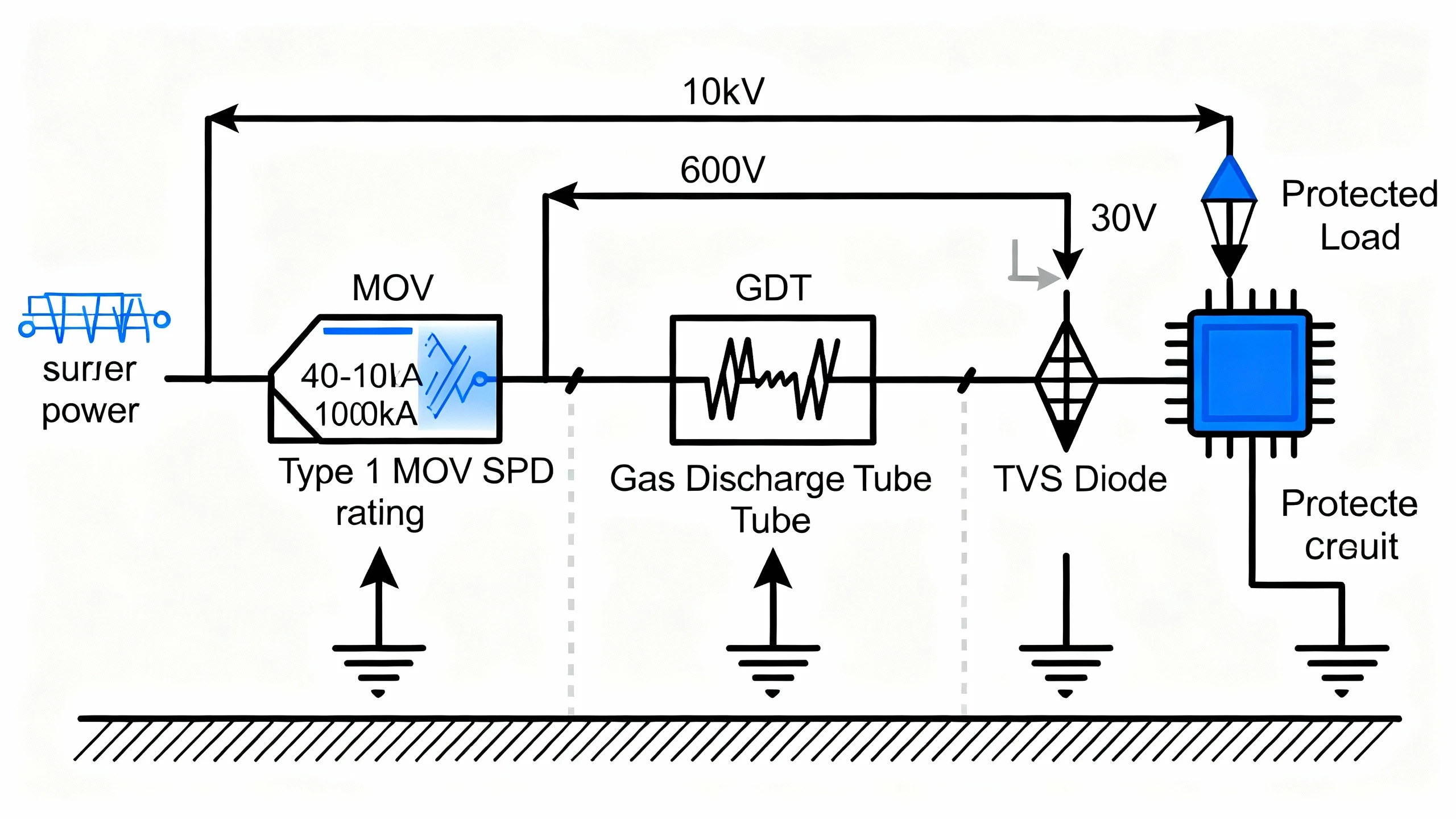
ပုံ ၅- ညှိနှိုင်းထားသော ကာကွယ်ရေးနည်းဗျူဟာကို သရုပ်ဖော်ထားသော ပရော်ဖက်ရှင်နယ် သုံးဆင့် လျှပ်စီးကာကွယ်ရေး ဗိသုကာပုံကြမ်း။ အဆင့် ၁ (မူလ) - ဝန်ဆောင်မှုအဝင်ပေါက်ရှိ Type 1 MOV SPD သည် အလွန်အမင်း လျှပ်စီးစွမ်းအင် (40-100 kA) ကို ကိုင်တွယ်ပြီး ဗို့အားကို 10+ kV မှ ~600V သို့ ထိန်းညှိပေးသည်။ အဆင့် ၂ (ဒုတိယ) - Gas Discharge Tube သည် ကျန်ရှိသော ဗို့အားမြင့် ယာယီလျှပ်စီးများကို လမ်းကြောင်းပြောင်းပေးပြီး arc mode လည်ပတ်မှုမှတစ်ဆင့် ဗို့အားကို ~30V သို့ လျှော့ချပေးသည်။ အဆင့် ၃ (နောက်ဆုံး) - TVS ဒိုင်အုတ်သည် အာရုံခံနိုင်သော semiconductor ဝန်များကို ကာကွယ်ရန် nanosecond တုံ့ပြန်မှုဖြင့် တင်းကျပ်သော clamping (<1.5× standoff voltage) ကို ပေးသည်။ အဆင့်တစ်ခုစီတွင် သင့်လျော်သော grounding နှင့် voltage ညှိနှိုင်းမှုတို့ ပါဝင်ပြီး upstream ကိရိယာများသည် downstream အစိတ်အပိုင်းများမတိုင်မီ စတင်အလုပ်လုပ်ကြောင်း သေချာစေကာ ကာကွယ်ရေး cascade တစ်လျှောက် လျှပ်စီးစွမ်းအင်ကို ဖြန့်ဝေပေးသည့် ရှင်းလင်းသော “handoff” အမှတ်များကို ဖန်တီးပေးသည်။ ဤအလွှာလိုက်ချဉ်းကပ်မှုသည် MOV (စွမ်းအင်မြင့်မားခြင်း)၊ GDT (capacitance နည်းပါးခြင်း) နှင့် TVS (တင်းကျပ်သော clamp) နည်းပညာများ၏ ဖြည့်စွက်အားသာချက်များကို အသုံးချသည်။.
အလွှာလိုက် ကာကွယ်မှု- နည်းပညာများကို ပေါင်းစပ်ခြင်း
အခိုင်မာဆုံး လျှပ်စီးကာကွယ်ရေး ဗိသုကာများသည် နည်းပညာတစ်ခုတည်းကို အားမကိုးပါ။ ယင်းအစား၊ ၎င်းတို့သည် ခြိမ်းခြောက်မှု spectrum ၏ မတူညီသော အပိုင်းတစ်ခုစီအတွက် အကောင်းဆုံးဖြစ်အောင် ပြုလုပ်ထားသော အဆင့်များစွာကို ညှိနှိုင်းဆောင်ရွက်ကြသည်။ ဤ “defense in depth” ချဉ်းကပ်မှုသည် MOV, GDT နှင့် TVS နည်းပညာများ၏ ဖြည့်စွက်အားသာချက်များကို အသုံးချသည်။.
အဘယ်ကြောင့် အလွှာလိုက် ကာကွယ်ရသနည်း။
စွမ်းအင် ဖြန့်ဝေခြင်း: TVS ဒိုင်အုတ်တစ်ခုတည်းသည် 10 kA လျှပ်စီးလျှပ်စီးကို မစုပ်ယူနိုင်သော်လည်း upstream ရှိ GDT သည် ထိုစွမ်းအင်၏ 99% ကို လမ်းကြောင်းပြောင်းပေးနိုင်ပြီး TVS သည် ကျန်ရှိသော စွမ်းအင်ကို ထိန်းညှိပေးနိုင်သည်။ အဆင့်တစ်ခုစီသည် ၎င်းလုပ်ဆောင်နိုင်သည့် အကောင်းဆုံးအရာကို ကိုင်တွယ်သည်။.
အရှိန်မြှင့်တင်ခြင်း: GDT သည် ionize လုပ်ရန် nanosecond ရာပေါင်းများစွာ ကြာသည်။ ထိုအချိန်အတွင်း downstream ရှိ အမြန် TVS သည် အစပိုင်း spike ကို ထိန်းညှိပေးနိုင်ပြီး အာရုံခံနိုင်သော ဝန်များ ပျက်စီးခြင်းမှ ကာကွယ်ပေးသည်။ GDT စတင်အလုပ်လုပ်သည်နှင့် ၎င်းသည် အမြောက်အမြား လျှပ်စီးကြောင်း လမ်းကြောင်းပြောင်းခြင်းကို တာဝန်ယူသည်။.
ဗို့အား ညှိနှိုင်းခြင်း: downstream ကိရိယာမတိုင်မီ upstream ကိရိယာသည် ပျက်စီးရမည်။ သင့်လျော်သော ရွေးချယ်မှုသည် ပထမအဆင့်သည် 600V တွင် စတင်အလုပ်လုပ်ကြောင်း သေချာစေပြီး ဒုတိယအဆင့် (150V အဆင့်သတ်မှတ်ထားသည်) သို့ ရောက်ရှိသည့်အရာကို ကန့်သတ်ထားပြီး နောက်ဆုံးဝန် (50V အဆင့်သတ်မှတ်ထားသည်) ကို ကာကွယ်ပေးသည်။.
အသုံးများသော အလွှာလိုက် ဗိသုကာများ
Telecom Interface (GDT + TVS):
- မူလအဆင့်: interface နယ်နိမိတ်ရှိ GDT သည် တိုက်ရိုက်လျှပ်စီးလက်ခြင်းနှင့် ဗို့အားမြင့် ပါဝါချို့ယွင်းမှုများကို ကိုင်တွယ်သည် (2-10 kV လျှပ်စီးများ၊ 20 kA အထိ)။.
- ဒုတိယအဆင့်: Low-capacitance TVS ဒိုင်အုတ်သည် transceiver IC (<30V) အတွက် ဘေးကင်းသောအဆင့်များသို့ ကျန်ရှိသော ယာယီလျှပ်စီးများကို ထိန်းညှိပေးသည်။.
- ညှိနှိုင်းဆောင်ရွက်ခြင်း: GDT sparkover သည် 400V တွင်ဖြစ်ပြီး TVS breakdown သည် 15V တွင်ဖြစ်ကာ transceiver ၏ အမြင့်ဆုံးအဆင့်သတ်မှတ်ချက်မှာ 12V ဖြစ်သည်။ TVS သည် GDT ionization နှောင့်နှေးမှုအတွင်း ကာကွယ်ပေးသည်။ GDT စတင်အလုပ်လုပ်သည်နှင့် ၎င်းသည် အမြောက်အမြား လျှပ်စီးကြောင်း တာဝန်ကို ယူဆသည်။.
Ethernet PoE (GDT + TVS + Inductor):
- မူလ: GDT သည် line-to-ground လျှပ်စီးလျှပ်စီးများကို လမ်းကြောင်းပြောင်းပေးသည်။.
- Series inductor: လျှပ်စီးတက်ချိန် (dV/dt) ကို နှေးကွေးစေပြီး GDT ကို ionize လုပ်ရန် အချိန်ပေးကာ downstream အဆင့်များသို့ လျှပ်စီးကြောင်းကို ကန့်သတ်ပေးသည်။.
- ဒုတိယ: differential pair တစ်ခုစီရှိ TVS ဒိုင်အုတ်များသည် Ethernet PHY (±8V max) ကို ကာကွယ်ရန် common-mode နှင့် differential-mode ယာယီလျှပ်စီးများကို ထိန်းညှိပေးသည်။.
စက်မှု AC Panel (MOV Primary + MOV Secondary):
- ဝန်ဆောင်မှု ဝင်ပေါက်: Type 1 MOV သည် 40-100 kA အဆင့်သတ်မှတ်ထားပြီး တိုက်ရိုက်လျှပ်စီးလက်ခြင်းကို ကိုင်တွယ်သည် (IEC 61643-11 အရ 1.2/50 µs ဗို့အား၊ 10/350 µs လျှပ်စီးကြောင်း ပုံစံများ)။.
- ဖြန့်ဖြူးရေး panel: Type 2 MOV သည် 20-40 kA အဆင့်သတ်မှတ်ထားပြီး အဆောက်အဦ ဝါယာကြိုးများမှတစ်ဆင့် တွဲဆက်ထားသော ကျန်ရှိသော လျှပ်စီးများကို ထိန်းညှိပေးသည်။.
- Load equipment: Type 3 SPD သို့မဟုတ် board-level TVS သည် နောက်ဆုံးအသုံးပြုသည့်နေရာ ကာကွယ်မှုကို ပေးသည်။.
PV Solar System (MOV DC + TVS):
- Array junction box: PV string output ရှိ DC-rated MOV (600-1000V) သည် လျှပ်စီးကြောင့်ဖြစ်သော လျှပ်စီးများကို ကိုင်တွယ်သည်။.
- Inverter ထည့်သွင်းမှု: TVS ဒိုင်အုတ်များသည် DC-DC converter နှင့် MPPT controller semiconductor များကိုကာကွယ်ပေးပြီး silicon ခံနိုင်ရည်ရှိသော level များတွင် clamping ပြုလုပ်ပေးသည်။.
အောင်မြင်သော ညှိနှိုင်းမှု၏ အဓိကအချက်မှာ ရှင်းလင်းသော “handoff” အမှတ်များကို ဖန်တီးပေးသော breakdown ဗို့အားများကို ရွေးချယ်ခြင်းနှင့် တစ်ဆင့်မှ ထွက်လာသော စွမ်းအင်သည် နောက်တစ်ဆင့်၏ အဆင့်သတ်မှတ်ချက်အတွင်း၌ ရှိနေကြောင်း အတည်ပြုခြင်းဖြစ်သည်။ VIOX ကဲ့သို့သော SPD စနစ်အစုံအလင် ထုတ်လုပ်သူများသည် ဤဒီဇိုင်းရှုပ်ထွေးမှုကို ဖယ်ရှားပေးသည့် စမ်းသပ်ပြီး ညှိနှိုင်းထားသော တပ်ဆင်မှုများကို မကြာခဏ ထုတ်ဝေလေ့ရှိသည်။.
နိဂုံး
surge protection အစိတ်အပိုင်းများကို ရွေးချယ်ခြင်းသည် “အကောင်းဆုံး” နည်းပညာကို ရှာဖွေခြင်းမဟုတ်ပါ - ၎င်းသည် ရူပဗေဒကို လိုအပ်ချက်များနှင့် ကိုက်ညီအောင် လုပ်ဆောင်ခြင်းဖြစ်သည်။ MOV များသည် ပါဝါဗို့အားများတွင် စွမ်းအင်မြင့်မားစွာ စုပ်ယူနိုင်ရန် ဇင့်အောက်ဆိုဒ် ကြွေထည်များကို အသုံးပြုသည်။ GDT များသည် အမြင့်ဆုံး current စွမ်းရည်ဖြင့် လိုင်းအားနည်းစေရန်အတွက် ဓာတ်ငွေ့ ionization ကို အသုံးချသည်။ TVS ဒိုင်အုတ်များသည် အထိခိုက်မခံသော အီလက်ထရွန်းနစ်ပစ္စည်းများကို အမြန်ဆုံးနှင့် တင်းကျပ်စွာ clamping ပြုလုပ်ရန် semiconductor avalanche ကို အသုံးပြုသည်။.
နည်းပညာတစ်ခုစီသည် အခြေခံ ကုန်သွယ်မှုတစ်ခုကို ကိုယ်စားပြုသည်-
- MOV များသည် စွမ်းအင်ကိုင်တွယ်မှုနှင့် ကုန်ကျစရိတ်အတွက် clamping ဗို့အားနှင့် သက်တမ်းကုန်ဆုံးမှုကို လဲလှယ်သည်။.
- GDT များသည် နှေးကွေးသော တုံ့ပြန်မှုနှင့် follow-current အန္တရာယ်အတွက် ultra-low capacitance နှင့် surge ခံနိုင်ရည်ကို လဲလှယ်သည်။.
- TVS ဒိုင်အုတ်များသည် အကန့်အသတ်ရှိသော စွမ်းအင်ပမာဏအတွက် အမြန်ဆုံးတုံ့ပြန်မှုနှင့် တင်းကျပ်သော ဗို့အားထိန်းချုပ်မှုကို လဲလှယ်သည်။.
ကျွန်ုပ်တို့ စစ်ဆေးပြီးသော လည်ပတ်မှုမူများတွင် အမြစ်တွယ်နေသော ဤကုန်သွယ်မှုများကို နားလည်ခြင်းသည် သင့်အသုံးချမှုတွင် အမှန်တကယ် အလုပ်ဖြစ်သော ကာကွယ်မှုကို သတ်မှတ်နိုင်စေပါသည်။ 5V data line ပေါ်ရှိ 600V MOV သည် ကာကွယ်ရန် ပျက်ကွက်လိမ့်မည်။ 10 kA လျှပ်စီးကြောင်းကို ရင်ဆိုင်နေရသော 40A TVS ဒိုင်အုတ်သည် ဆိုးရွားစွာ ပျက်ကွက်လိမ့်မည်။ impedance နည်းသော DC supply ပေါ်ရှိ GDT သည် အဖျက်အမှောက်ဖြစ်စေသော follow-current conduction သို့ ရောက်ရှိသွားနိုင်သည်။.
ရှုပ်ထွေးသော တပ်ဆင်မှုများအတွက်၊ အလွှာလိုက်ကာကွယ်မှုသည် နည်းပညာများစွာကို ညှိနှိုင်းပေးပြီး တစ်ခုစီကို အကောင်းဆုံးလုပ်ဆောင်နိုင်သည့်နေရာတွင် နေရာချထားပေးသည်။ GDT သည် အလုံးလိုက်စွမ်းအင်ကို စုပ်ယူပြီး MOV သည် ပါဝါအဆင့် surge များကို ကိုင်တွယ်ကာ TVS သည် semiconductor load များအတွက် နောက်ဆုံးအဆင့် clamping ကို ပေးသည်။.
သင်သည် IEC 61643-11 အရ 100 kA အဆင့်သတ်မှတ်ထားသော ပါဝါဖြန့်ဖြူးရေး SPD ကို ဒီဇိုင်းဆွဲသည်ဖြစ်စေ၊ sub-2 pF loading ပါသော Gigabit Ethernet interface ကို ကာကွယ်သည်ဖြစ်စေ၊ သို့မဟုတ် 3.3V FPGA I/O ကို ကာကွယ်သည်ဖြစ်စေ၊ ဆုံးဖြတ်ချက်မူဘောင်သည် အတူတူပင်ဖြစ်သည်- စက်ပစ္စည်းရူပဗေဒကို circuit လိုအပ်ချက်များနှင့် ကိုက်ညီအောင်ပြုလုပ်ပါ၊ ခြိမ်းခြောက်မှုပုံစံများနှင့်အညီ အဆင့်သတ်မှတ်ချက်များကို စစ်ဆေးပြီး နည်းပညာတစ်ခုတည်းက spectrum အပြည့်အစုံကို မကာကွယ်နိုင်သည့်အခါ အဆင့်များကို ညှိနှိုင်းပါ။.
VIOX Electric အကြောင်း: surge protection စက်ပစ္စည်းများ၏ ဦးဆောင်ထုတ်လုပ်သူအနေဖြင့် VIOX သည် လူနေအိမ်၊ စီးပွားဖြစ်နှင့် စက်မှုလုပ်ငန်းသုံးများအတွက် ပြည့်စုံသော MOV, GDT နှင့် TVS ဖြေရှင်းနည်းများကို ပေးပါသည်။ ကျွန်ုပ်တို့၏ အင်ဂျင်နီယာအဖွဲ့သည် ညှိနှိုင်းထားသော ကာကွယ်မှုစနစ်များအတွက် application support ကို ပေးပါသည်။ ဝင်ရောက်ကြည့်ရှုပါ www.viox.com သို့မဟုတ် သတ်မှတ်ချက်အကူအညီအတွက် ကျွန်ုပ်တို့၏ နည်းပညာဆိုင်ရာ အရောင်းအဖွဲ့ထံ ဆက်သွယ်ပါ။.