مقدمه
在为电气系统指定浪涌保护时,工程师面临三种核心技术的基本选择:金属氧化物压敏电阻(MOV)、气体放电管(GDT)和瞬态电压抑制(TVS)二极管。每种技术都基于不同的物理原理,提供独特的性能特征——MOV利用非线性陶瓷电阻,GDT利用气体电离,TVS二极管则利用半导体雪崩击穿。MOV选择并非在于寻找“最佳”技术,而在于根据应用需求匹配基本的权衡取舍。一种在交流电源配电中表现出色的MOV,在高速数据线上可能会发生灾难性故障。一种适用于电信接口的GDT,对于5V直流电源轨则不合适。一种在板级I/O保护中理想的TVS二极管,在暴露于雷电的户外电路上可能会不堪重负。.
本文将从基本原理出发,逐一审视每种技术,解释其性能差异背后的物理原理,并在响应时间、钳位电压、能量处理能力、电容、老化行为和成本方面提供量化比较。无论您是设计配电系统、保护通信接口,还是协调多级保护,理解这些根本差异将帮助您选择真正能提供保护的元件,而不仅仅是满足采购要求。.
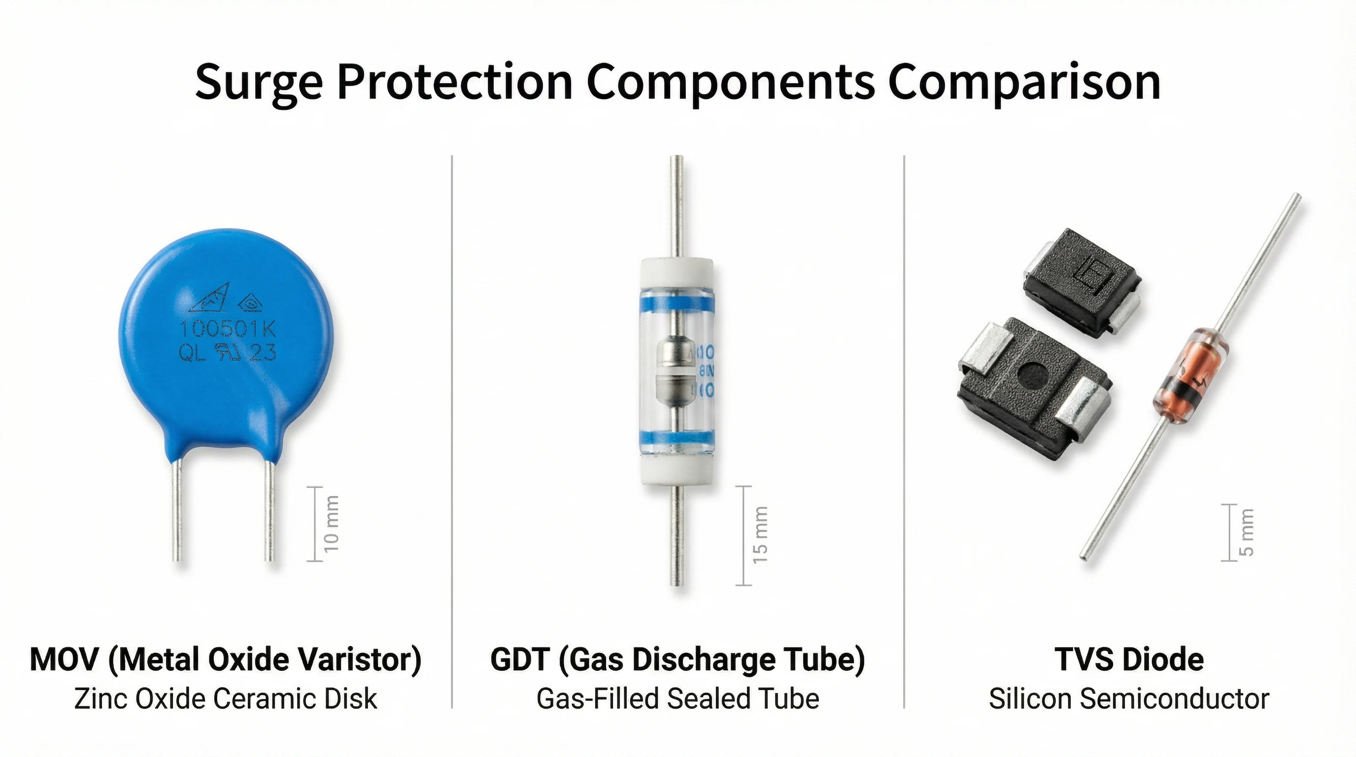
图0:三种浪涌保护技术的实物对比。左图:MOV(金属氧化物压敏电阻)展示了典型的蓝色氧化锌陶瓷圆盘和径向引线——其物理尺寸随额定电压(圆盘厚度)和电流容量(圆盘直径)而变化。中图:GDT(气体放电管)显示了包含惰性气体和电极的圆柱形密封玻璃/陶瓷外壳——其密封结构确保了稳定的火花放电特性。右图:TVS二极管展示了从紧凑型SMD封装(0402,SOT-23)到较大的通孔封装(DO-201,DO-218)的各种半导体封装形式——硅芯片尺寸决定了脉冲功率额定值。这些显著的物理差异反映了根本不同的工作原理:陶瓷晶界结(MOV)、气体电离等离子体(GDT)和半导体雪崩击穿(TVS)。 اس پی دی, MOV(金属氧化物压敏电阻):结构与工作原理.
金属氧化物压敏电阻是一种陶瓷半导体器件,其电阻值随电压升高而急剧下降。这种压敏特性使其像一个自动电压钳——在浪涌期间大量导通,而在正常工作时几乎不可见。.
内部结构
MOV由氧化锌(ZnO)晶粒与少量铋、钴、锰和其他金属氧化物烧结而成。其神奇之处在于晶界。相邻ZnO晶粒之间的每个边界都形成一个微观的肖特基势垒——本质上是一个微小的背对背二极管结。单个MOV圆盘包含数百万个这样的微结,它们以复杂的三维串并联网络连接。.
器件的整体特性源于这种微观结构。圆盘厚度决定了工作电压(串联的晶界越多,额定电压越高)。圆盘直径决定了电流能力(并联路径越多,浪涌电流越大)。这就是为什么MOV数据手册会规定每毫米厚度的压敏电压,以及为什么用于配电的高能量MOV在物理上是大型块状或圆盘组件。
当电压低于压敏电压(Vᵥ)时,晶界结保持在耗尽模式,器件仅吸收微安级的漏电流。当浪涌将电压驱动至Vᵥ以上时,结通过量子隧穿和雪崩倍增发生击穿。电阻从兆欧级骤降至欧姆级,MOV将浪涌电流旁路至地。.
这种转变本质上是快速的——在材料层面为亚纳秒级。标准目录中的MOV可实现低于25纳秒的响应时间,其主要限制因素是引线电感和封装几何结构,而非ZnO的物理特性。其电压-电流特性是高度非线性的,通常用公式 I = K·Vᵅ 描述,其中非线性系数α的范围为25至50(相比之下,线性电阻的α = 1)。.
اصل عملیاتی
关键规格与特性.
能量处理能力.
Key Specifications and Behavior
Energy Handling: MOVs excel at absorbing surge energy. Manufacturers rate energy capability using 2-millisecond rectangular pulses and surge current using the standard 8/20 µs waveform. Block MOVs for power distribution can handle 10,000 to 100,000 amperes of surge current in single events.
Aging and Degradation: Repeated surge exposure causes cumulative microstructural damage. The varistor voltage shifts downward, leakage current increases, and clamping performance degrades. Heavy overloads can puncture grain boundaries, creating permanent conductive paths. For this reason, datasheets specify derating factors for repetitive surges, and critical installations should monitor MOV leakage current as a maintenance parameter.
برنامه های کاربردی معمولی: AC mains surge protection, power distribution panels, industrial motor drives, heavy equipment, and any application requiring high energy absorption with fast (nanosecond) response.
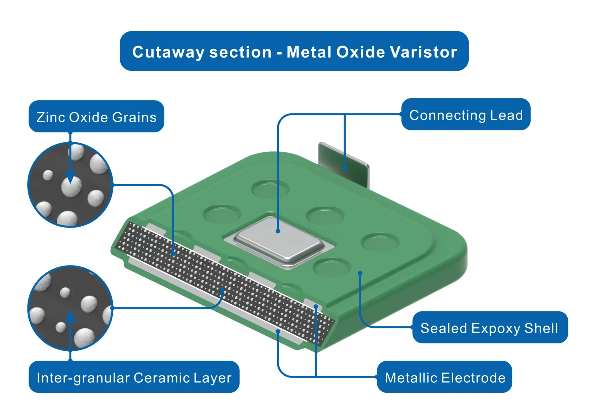
Figure 1: MOV cutaway section showing zinc oxide (ZnO) grains embedded in ceramic matrix with inter-granular boundaries (magnified inset). Each grain boundary forms a microscopic Schottky barrier, creating millions of micro-junctions in series-parallel configuration. The disk’s physical dimensions—thickness determines voltage rating (more boundaries in series), diameter determines current capability (more parallel paths)—directly control surge protection performance.
GDT (Gas Discharge Tube): Structure and Operating Principle
The Gas Discharge Tube takes a fundamentally different approach: instead of clamping voltage with nonlinear resistance, it creates a temporary short circuit when voltage exceeds a threshold. This “crowbar” action diverts surge current through ionized gas rather than solid-state materials.
器件的整体特性源于这种微观结构。圆盘厚度决定了工作电压(串联的晶界越多,额定电压越高)。圆盘直径决定了电流能力(并联路径越多,浪涌电流越大)。这就是为什么MOV数据手册会规定每毫米厚度的压敏电压,以及为什么用于配电的高能量MOV在物理上是大型块状或圆盘组件。
A GDT consists of two or three electrodes sealed inside a ceramic or glass envelope filled with inert gas (typically a mixture of argon, neon, or xenon at sub-atmospheric pressure). The electrode gap and gas composition determine the breakdown voltage. The hermetic seal is critical—any contamination or pressure change would alter breakdown characteristics.
Three-electrode GDTs are common in telecom applications, providing line-to-line and line-to-ground protection in a single component. Two-electrode versions serve simpler line-to-ground configurations. The electrodes are often coated with materials that reduce the breakdown voltage and stabilize arc formation.
اصل عملیاتی
Under normal conditions, the gas is non-conductive and the GDT presents near-infinite impedance (>10⁹ Ω) with extremely low capacitance—typically below 2 picofarads. When a transient voltage exceeds the spark-over voltage, the electric field ionizes the gas. Free electrons accelerate and collide with gas atoms, liberating more electrons in an avalanche process. Within a fraction of a microsecond, a conductive plasma channel forms between electrodes.
Once ionized, the GDT enters arc mode. Voltage across the device collapses to a low arc voltage—typically 10-20 volts regardless of the initial breakdown voltage. The device now acts as a near-short, diverting surge current through the plasma. The arc persists until current drops below the “glow-to-arc transition current,” typically tens of milliamperes.
This crowbar behavior creates a critical design consideration: if the protected circuit can source sufficient “follow current” above the glow threshold, the GDT may latch in conduction even after the transient ends. This is why GDTs on AC mains require series resistance or coordination with upstream breakers. On low-impedance DC supplies, follow-current latching can be catastrophic.
Key Specifications and Behavior
Surge Current Capability: GDTs handle extremely high surge currents—typical telecom-grade devices are rated for 10,000 to 20,000 amperes (8/20 µs waveform) with multi-shot endurance. This high capacity comes from the distributed nature of the plasma channel rather than localized solid-state junctions.
Capacitance: The defining advantage of GDTs is their sub-2 pF capacitance, making them transparent to high-speed signals. This is why they dominate telecom line protection: xDSL, cable broadband, and Gigabit Ethernet can’t tolerate the capacitance of MOVs or many TVS devices.
زمان پاسخ: GDTs are slower than solid-state devices. Breakdown typically occurs within hundreds of nanoseconds to a few microseconds, depending on the voltage overshoot (higher dV/dt accelerates ionization). For fast transients on sensitive electronics, GDTs are often paired with faster clamps in a coordinated protection scheme.
Stability and Lifespan: Quality GDTs exhibit excellent long-term stability. ITU-T K.12 and IEEE C62.31 test methods verify performance over thousands of surge cycles. UL-recognized telecom GDTs demonstrate minimal parameter shift over decades of service.
برنامه های کاربردی معمولی: Telecom line protection (xDSL, cable, fiber optics), high-speed Ethernet interfaces, RF and antenna inputs, and any application where minimal line loading is essential and the surge source impedance is high enough to prevent follow-current latching.
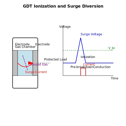
Figure 2: Gas Discharge Tube (GDT) construction and operating behavior. Left diagram shows internal structure: hermetically sealed gas chamber with electrode gap and inert gas fill (argon/neon). Right graph illustrates ionization response—when transient voltage exceeds spark-over threshold, gas ionizes creating conductive plasma channel, voltage collapses to arc mode (~10-20V), and surge current diverts through the plasma until current drops below glow-to-arc transition threshold.
TVS Diode: Structure and Operating Principle
Transient Voltage Suppressor diodes are silicon avalanche devices engineered specifically for surge clamping. They combine the fastest response times with the lowest clamping voltages available in surge protection components, making them the preferred choice for protecting sensitive semiconductor circuits.
器件的整体特性源于这种微观结构。圆盘厚度决定了工作电压(串联的晶界越多,额定电压越高)。圆盘直径决定了电流能力(并联路径越多,浪涌电流越大)。这就是为什么MOV数据手册会规定每毫米厚度的压敏电压,以及为什么用于配电的高能量MOV在物理上是大型块状或圆盘组件。
A TVS diode is essentially a specialized Zener diode optimized for high pulse power rather than voltage regulation. The silicon die features a heavily doped P-N junction designed to enter avalanche breakdown at a precise voltage. Die area is much larger than equivalent Zener regulators to handle the peak currents of surge events—hundreds of amperes in submicrosecond pulses.
اصل عملیاتی
Under normal operating voltage, the TVS diode operates in reverse bias with only nanoampere-level leakage. When a transient exceeds the reverse breakdown voltage (V_BR), the silicon junction enters avalanche multiplication. Impact ionization generates a flood of electron-hole pairs, and junction resistance collapses. The device clamps voltage at the breakdown level plus the dynamic resistance times the surge current.
The physics is purely solid-state with no mechanical motion, gas ionization, or material phase change. This enables response times in the nanosecond range—sub-1 ns for the bare silicon, though package inductance typically pushes effective response to 1-5 ns for practical devices. The voltage-current characteristic is very steep (low dynamic resistance), providing tight clamping.
Key Specifications and Behavior
Pulse Power Ratings: TVS manufacturers specify power capacity using standardized pulse widths (typically 10/1000 µs exponential waveforms). Common product families offer 400W, 600W, 1500W, or 5000W pulse ratings. Peak current capability is calculated from pulse power and clamping voltage—a 600W device with 15V clamp handles about 40A peak.
Clamping Performance: TVS diodes offer the lowest clamping voltages of any surge protection technology. The ratio of clamping voltage to standoff voltage (V_C/V_WM) is typically 1.3 to 1.5, compared to 2.0-2.5 for MOVs. This tight control is critical for protecting 3.3V logic, 5V USB, 12V automotive circuits, and other voltage-sensitive loads.
Capacitance: TVS capacitance varies widely with device construction. Standard junction TVS diodes can exhibit hundreds of picofarads, which loads high-speed data lines. Low-capacitance TVS families engineered for HDMI, USB 3.0, Ethernet, and RF use specialized junction geometries and achieve sub-5 pF per line.
Aging and Reliability: Unlike MOVs, TVS diodes exhibit minimal performance drift under rated pulse stress. The silicon junction doesn’t degrade cumulatively from repeated surges within ratings. Failure modes are typically open-circuit (junction annihilation) or short-circuit (metallization fusing), both of which occur only under extreme overload well beyond ratings.
برنامه های کاربردی معمولی: Board-level circuit protection (I/O ports, power rails), USB and HDMI interfaces, automotive electronics, DC power supplies, communication data lines, and any application requiring fast response and tight voltage clamping for semiconductor loads.
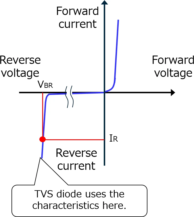
Figure 3: TVS diode voltage-current (I-V) characteristic curve showing semiconductor avalanche operation. Under normal voltage (V_WM standoff region), device maintains high impedance with nanoampere leakage. When transient exceeds reverse breakdown voltage (V_BR), silicon P-N junction enters avalanche multiplication—junction resistance collapses and device clamps voltage at V_C (breakdown voltage plus dynamic resistance × surge current). The steep curve (low dynamic resistance) provides tight voltage control critical for protecting semiconductor loads.
Clamping vs Crowbar: Two Protection Philosophies
The fundamental difference between these technologies lies in their protection philosophy. MOVs and TVS diodes are clamping devices—they limit voltage to a specific level proportional to surge current. GDTs are crowbar devices—they create a short circuit that collapses voltage to a low residual level regardless of current magnitude.
Clamping behavior (MOV and TVS): As surge current increases, clamping voltage rises according to the device’s nonlinear V-I curve. A MOV rated 275V RMS might clamp at 750V for a 1 kA surge but rise to 900V at 5 kA. A TVS diode rated 15V standoff might clamp at 24V for 10A but reach 26V at 20A. The protected load sees a voltage determined by surge amplitude and device characteristics.
Crowbar behavior (GDT): Once breakdown occurs, the GDT enters arc mode and voltage collapses to 10-20V regardless of whether surge current is 100A or 10,000A. This provides excellent protection once triggered, but the initial spark-over can allow a voltage spike before ionization completes. This is why sensitive loads behind GDTs often need a secondary fast clamp.
Each philosophy suits different applications. Clamping devices protect by limiting voltage exposure. Crowbar devices protect by diverting current. Clamping works when the protected circuit can tolerate the clamp voltage. Crowbar works when the surge source has high enough impedance that shorting the line doesn’t damage upstream equipment or cause follow-current problems.
MOV vs GDT vs TVS: Side-by-Side Comparison
The table below quantifies the key performance differences across these three surge protection technologies:
| پارامتر | MOV (Metal Oxide Varistor) | GDT (Gas Discharge Tube) | دیود TVS |
| اصل عملیاتی | Voltage-dependent nonlinear resistance (ZnO grain boundaries) | Gas ionization crowbar | Semiconductor avalanche breakdown |
| مکانیسم حفاظت | Clamping | Crowbar | Clamping |
| زمان پاسخ | <25 ns (typical catalog parts) | 100 ns – 1 µs (voltage-dependent) | 1-5 ns (package-limited) |
| Clamping/Arc Voltage | 2.0-2.5 × MCOV | 10-20 V (arc mode) | 1.3-1.5 × V_standoff |
| Surge Current (8/20 µs) | 400 A – 100 kA (size-dependent) | 5 kA – 20 kA (telecom-grade) | 10 A – 200 A (600W family ~40A) |
| Energy Handling | Excellent (100-1000 J) | Excellent (distributed plasma) | Moderate (limited by junction) |
| Capacitance | 50-5000 pF (area-dependent) | <2 pF | 5-500 pF (construction-dependent) |
| Aging Behavior | Degrades with surge cycles; V_n drifts down | Stable over thousands of surges | Minimal drift within ratings |
| Failure Mode | Degradation → short or open | Short (arc sustaining) | Open or short (catastrophic only) |
| Follow-Current Risk | Low (self-extinguishing) | High (requires external limiting) | None (solid-state) |
| Typical Voltage Range | 18V RMS – 1000V RMS | 75V – 5000V DC sparkover | 3.3V – 600V standoff |
| Cost (Relative) | Low ($0.10 – $5) | Low-Medium ($0.50 – $10) | Low-Medium ($0.20 – $8) |
| استانداردها | IEC 61643-11, UL 1449 | ITU-T K.12, IEEE C62.31 | IEC 61643-11, UL 1449 |
| Primary Applications | AC mains, power distribution, industrial | Telecom lines, high-speed data, antenna | Board-level I/O, DC supplies, automotive |
Key Takeaways from the Comparison
MOV ها offer the best balance of energy handling, fast response, and cost for power-level surges. They dominate AC mains protection but suffer from capacitance loading on high-frequency circuits and cumulative aging under repeated stress.
GDTs excel where minimal line loading is critical and surge current capability must be maximized. Their ultra-low capacitance makes them irreplaceable in telecom and RF applications, but slower response and follow-current risk require careful circuit design.
TVS diodes provide the fastest, tightest clamping for sensitive electronics. They are the only practical choice for protecting semiconductor I/O at voltages below 50V, but limited energy capacity means they can’t handle the lightning-level surges that MOVs and GDTs routinely absorb.
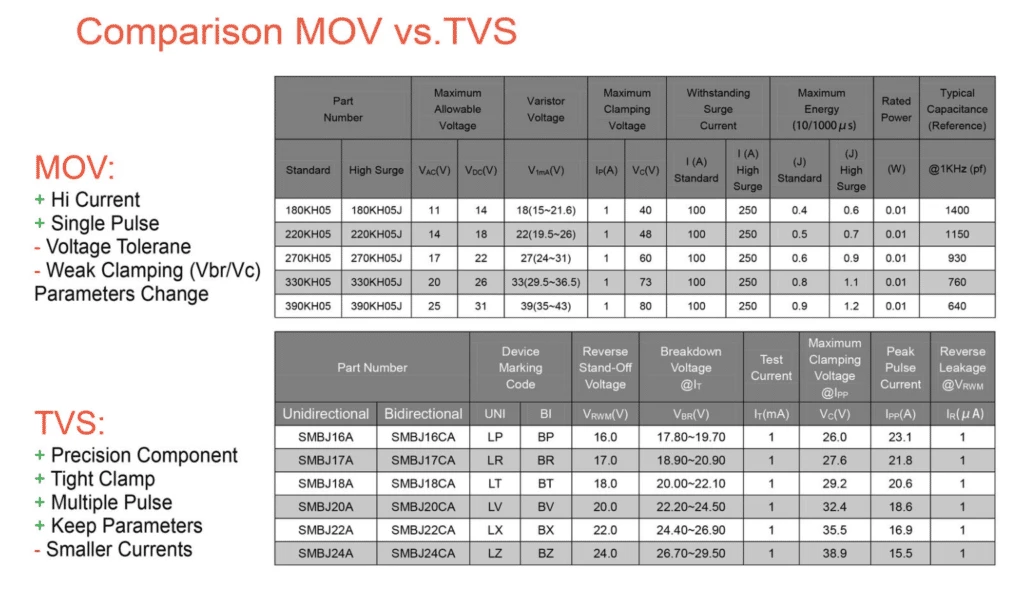
Figure 4: Professional comparison chart contrasting MOV (Metal Oxide Varistor) and TVS (Transient Voltage Suppressor) technologies across key specifications. MOVs exhibit higher clamping voltage ratios (2.0-2.5× MCOV) with excellent energy absorption for power-level surges, while TVS diodes deliver tighter voltage control (1.3-1.5× standoff) with faster response (<5 ns) for semiconductor protection. The table includes voltage ratings, surge current capabilities, and typical part number examples demonstrating the complementary performance envelopes of each technology.
Technology Selection Guide: When to Use Each
Choosing the right surge protection technology depends on matching device characteristics to circuit requirements. Here’s a decision framework:
Use MOV When:
- Circuit voltage is AC mains or high-voltage DC (>50V): MOVs are available in voltage ratings from 18V RMS to over 1000V, perfectly matching residential (120/240V), commercial (277/480V), and industrial power distribution.
- Surge energy is high: Lightning-induced surges, utility switching transients, and motor inrush produce energy levels (hundreds to thousands of joules) that only MOVs can absorb economically.
- Response time <25 ns is acceptable: Most power electronics and industrial equipment tolerate MOV response speed.
- Capacitance loading is acceptable: At power frequencies (50/60 Hz), even 1000 pF capacitance is negligible.
- Cost is constrained: MOVs offer the lowest cost per joule of protection.
Avoid MOVs when protecting high-speed communication lines (capacitance loading), low-voltage semiconductor circuits (clamping voltage too high), or applications requiring guaranteed no-drift performance over decades (aging concerns).
Use GDT When:
- Line loading must be minimal (<2 pF): xDSL modems, cable broadband, Gigabit Ethernet, RF receivers, and antenna inputs cannot tolerate the capacitance of MOVs or standard TVS devices.
- Surge current capability must be maximized: Telecom central offices, cell towers, and outdoor installations face repeated high-amplitude lightning surges that exceed TVS ratings.
- Protected circuit has high source impedance: Telephone lines (600Ω), antenna feedlines (50-75Ω), and data cables can safely be crowbarred without excessive follow-current.
- Operating voltage is high (>100V): GDTs are available with sparkover voltages from 75V to 5000V, covering telecom voltages, PoE (Power over Ethernet), and high-voltage signaling.
Avoid GDTs when protecting low-impedance DC power supplies (follow-current risk), circuits requiring fastest response (<100 ns critical), or voltage-sensitive loads that can’t tolerate the initial spark-over spike (needs secondary clamping).
Use TVS Diode When:
- Clamping voltage must be tightly controlled: 3.3V logic, 5V USB, 12V automotive circuits, and other semiconductor loads require clamping within 20-30% of nominal voltage—only TVS diodes deliver this.
- Response time must be fastest (<5 ns): Protecting high-speed processors, FPGAs, and sensitive analog circuits demands nanosecond response.
- Circuit voltage is low to medium (<100V): TVS families cover everything from 3.3V data lines to 48V telecom supplies.
- Aging/drift cannot be tolerated: Medical devices, aerospace, and safety-critical systems require predictable, stable protection over product lifetime.
- Board space is limited: SMT TVS devices in 0402 or SOT-23 packages fit where MOVs and GDTs cannot.
Avoid TVS diodes when surge energy exceeds pulse power rating (typical 600W device absorbs only ~1 joule), surge current exceeds peak rating (40A typical for 600W at 15V), or cost per channel becomes prohibitive in multi-line systems.
ماتریس تصمیمگیری
| کاربرد | Primary Technology | منطق |
| AC mains panel protection | MOV (Type 1/2 SPD) | High energy, 120-480V, cost-effective |
| Telecom line interface | GDT + TVS (staged) | GDT absorbs energy, TVS clamps residual |
| USB 2.0 / 3.0 data lines | Low-cap TVS | Fast edges, 5V supply, <5 pF required |
| Ethernet (10/100/1000 Base-T) | GDT (primary) + low-cap TVS | Minimal loading, high surge exposure |
| 24V DC industrial I/O | TVS | Tight clamp, fast response, no aging |
| PV solar DC input | MOV (DC-rated) | High voltage (600-1000V), high energy |
| Automotive 12V circuits | TVS | Load dump protection, tight clamp at 24-36V |
| RF antenna input | GDT | Sub-2 pF, high power handling |
| 3.3V FPGA power rail | TVS (low-cap) | 6-8V clamp, <1 ns response critical |
This matrix is a starting point. Complex installations often combine technologies in layered protection schemes, leveraging the strengths of each stage.
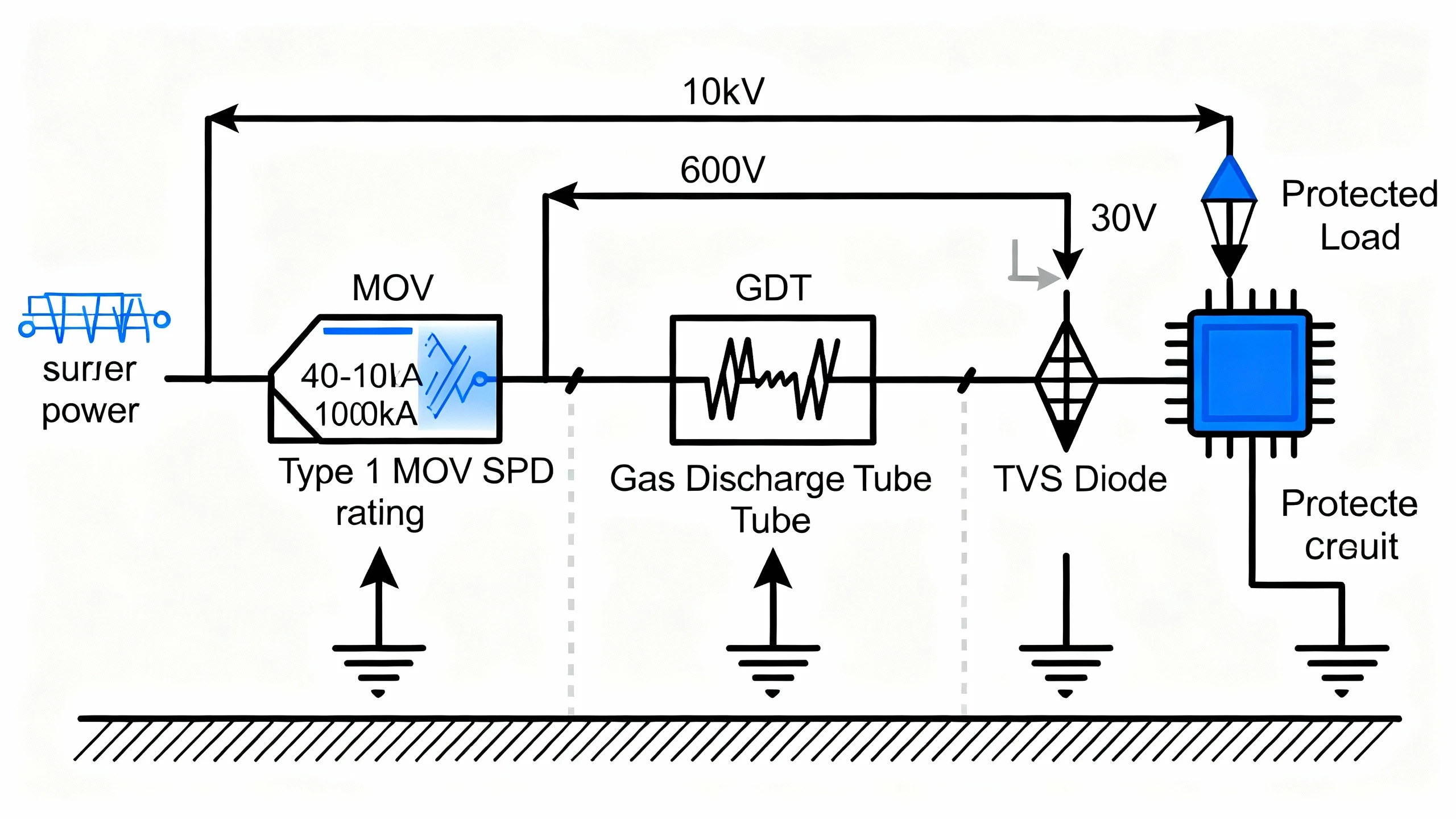
Figure 5: Professional three-stage surge protection architecture diagram illustrating coordinated protection strategy. Stage 1 (Primary): Type 1 MOV SPD at service entrance handles extreme surge energy (40-100 kA) and clamps voltage from 10+ kV to ~600V. Stage 2 (Secondary): Gas Discharge Tube diverts residual high-voltage transients and reduces voltage to ~30V through arc mode operation. Stage 3 (Final): TVS diode provides tight clamping (<1.5× standoff voltage) with nanosecond response to protect sensitive semiconductor loads. Each stage features proper grounding and voltage coordination to ensure upstream devices trigger before downstream components, creating clear “handoff” points that distribute surge energy across the protection cascade. This layered approach leverages the complementary strengths of MOV (high energy), GDT (low capacitance), and TVS (tight clamp) technologies.
Layered Protection: Combining Technologies
The most robust surge protection architectures don’t rely on a single technology. Instead, they coordinate multiple stages, each optimized for a different portion of the threat spectrum. This “defense in depth” approach leverages the complementary strengths of MOV, GDT, and TVS technologies.
Why Layer Protection?
Energy distribution: A single TVS diode can’t absorb a 10 kA lightning surge, but a GDT upstream can divert 99% of that energy, leaving the TVS to clamp the residual. Each stage handles what it does best.
Speed optimization: A GDT takes hundreds of nanoseconds to ionize. During that time, a fast TVS downstream can clamp the initial spike, preventing damage to sensitive loads. Once the GDT fires, it takes over bulk current diversion.
Voltage coordination: The upstream device must break down before the downstream device. Proper selection ensures the first stage conducts at, say, 600V, limiting what reaches the second stage (rated 150V), which in turn protects the final load (rated 50V).
Common Layered Architectures
Telecom Interface (GDT + TVS):
- Primary stage: GDT at the interface boundary handles direct lightning strikes and high-voltage power faults (2-10 kV surges, up to 20 kA).
- Secondary stage: Low-capacitance TVS diode clamps residual transients to safe levels for the transceiver IC (<30V).
- هماهنگی: GDT sparkover at 400V, TVS breakdown at 15V, transceiver maximum rating 12V. The TVS protects during GDT ionization delay; once GDT fires, it assumes bulk current duty.
Ethernet PoE (GDT + TVS + Inductor):
- Primary: GDT diverts line-to-ground lightning surges.
- Series inductor: Slows surge rise time (dV/dt), giving GDT time to ionize and limiting current into downstream stages.
- Secondary: TVS diodes on each differential pair clamp common-mode and differential-mode transients to protect the Ethernet PHY (±8V max).
Industrial AC Panel (MOV Primary + MOV Secondary):
- ورودی سرویس: Type 1 MOV rated 40-100 kA handles direct lightning (1.2/50 µs voltage, 10/350 µs current waveforms per IEC 61643-11).
- Distribution panel: Type 2 MOV rated 20-40 kA clamps residual surges that couple through building wiring.
- Load equipment: Type 3 SPD or board-level TVS provides final point-of-use protection.
PV Solar System (MOV DC + TVS):
- Array junction box: DC-rated MOV (600-1000V) on PV string output handles lightning-induced surges.
- Inverter input: TVS diodes protect DC-DC converter and MPPT controller semiconductors, clamping at levels the silicon can survive.
The key to successful coordination is selecting breakdown voltages that create clear “handoff” points and verifying that let-through energy from one stage remains within the rating of the next stage. Manufacturers of complete SPD systems (like VIOX) often publish tested, coordinated assemblies that eliminate this design complexity.
نتيجه گيری
Selecting surge protection components is not about finding the “best” technology—it’s about matching physics to requirements. MOVs leverage zinc oxide ceramics to absorb high energy at power voltages. GDTs exploit gas ionization to achieve minimal line loading with maximum current capability. TVS diodes harness semiconductor avalanche for the fastest, tightest clamping of sensitive electronics.
Each technology represents a fundamental trade-off:
- MOVs trade higher clamping voltage and aging for excellent energy handling and cost.
- GDTs trade slower response and follow-current risk for ultra-low capacitance and surge endurance.
- TVS diodes trade limited energy capacity for fastest response and tightest voltage control.
Understanding these trade-offs—rooted in the operating principles we’ve examined—enables you to specify protection that actually works in your application. A 600V MOV on a 5V data line will fail to protect. A 40A TVS diode facing a 10 kA lightning surge will fail catastrophically. A GDT on a low-impedance DC supply may latch into destructive follow-current conduction.
For complex installations, layered protection coordinates multiple technologies, positioning each where it performs best. The GDT absorbs bulk energy, the MOV handles power-level surges, and the TVS delivers final-stage clamping for semiconductor loads.
Whether you’re designing a power distribution SPD rated for 100 kA per IEC 61643-11, protecting a Gigabit Ethernet interface with sub-2 pF loading, or safeguarding 3.3V FPGA I/O, the decision framework is the same: match device physics to circuit requirements, verify ratings against threat waveforms, and coordinate stages when a single technology can’t cover the full spectrum.
درباره ویوکس الکتریک: As a leading manufacturer of surge protection devices, VIOX offers comprehensive MOV, GDT, and TVS solutions for residential, commercial, and industrial applications. Our engineering team provides application support for coordinated protection systems. Visit www.viox.com or contact our technical sales team for specification assistance.